In the world of advanced packaging conversations about 2.5D, 3D ICs, and chiplet integration, wire bonding remains the unsung hero of semiconductor packaging. This foundational technology creates the critical electrical bridge between silicon dies and the external world, enabling billions of devices to function reliably every day.
Understanding Wire Bonding: The Foundation of Chip Connectivity
While the semiconductor industry pushes toward advanced packaging technologies, wire bonding remains the backbone of chip-to-package interconnection. This mature technology connects the microscopic world of silicon circuits to the macroscopic realm of electronic systems through incredibly thin metallic wires.
Wire Bonding Process
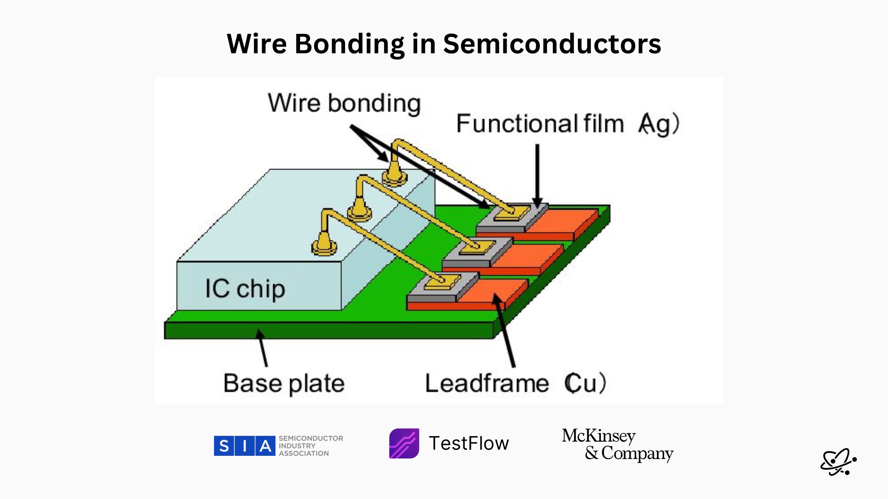
Ultrathin gold, copper, or aluminum wires (15-50 micrometers diameter) are precisely welded between bonding pads on the IC chip and corresponding pads on the leadframe or substrate. This creates the electrical pathway for signals, power, and ground connections.
Proven reliability with decades of manufacturing experience and optimization
Package Integration
The silicon die is mounted on a base structure (leadframe or substrate) that provides mechanical support and thermal management. Wire bonds then create the electrical interface between the isolated chip and the package's external connections.
Cost-effective solution suitable for high-volume manufacturing
Anatomy of Wire Bonding: Breaking Down the Components
Understanding the wire bonding process requires examining each component and how they work together to create reliable electrical connections.
IC Chip & Base Plate
The silicon die contains the actual circuitry and is mounted on a base structure that provides mechanical stability and thermal management. Bonding pads on the chip's periphery serve as connection points for wire bonds.
Wire Bonds
Ultrathin metallic wires create the electrical pathway between chip and package. Gold wires offer excellent corrosion resistance, while copper provides better electrical and thermal conductivity at lower cost.
Leadframe & Functional Film
The leadframe (typically copper) routes signals from the chip to external package pins. Silver-based functional films improve conductivity and bonding strength at connection points.
The Building Infrastructure Analogy
IC Chip = Workstation in a Building
The silicon die is like a sophisticated workstation with powerful computing capabilities, but it's isolated from the outside world without proper connections.
Wire Bonds = Power and Data Cables
Wire bonds are the essential infrastructure cables connecting the workstation to the building's power grid, internet, and communication systems. Without them, the system remains isolated and non-functional.
Wire Bonding Technologies: Materials and Methods
Different wire bonding technologies have evolved to meet specific performance, cost, and reliability requirements across various applications.
| Wire Material | Diameter Range | Key Benefits | Typical Applications |
|---|---|---|---|
| Gold (Au) | 15-50 μm | Excellent corrosion resistance, reliable bonding | High-reliability applications, aerospace, medical |
| Copper (Cu) | 20-75 μm | Lower cost, better electrical/thermal conductivity | Consumer electronics, automotive, power devices |
| Aluminum (Al) | 25-100 μm | Low cost, good for high-current applications | Power semiconductors, industrial applications |
Where Wire Bonding Dominates
Despite the emergence of advanced packaging technologies, wire bonding continues to be the preferred choice for numerous applications due to its proven reliability and cost-effectiveness.
High-Volume Applications
- • Consumer electronics (smartphones, tablets, wearables)
- • Automotive microcontrollers and sensors
- • Power management ICs
- • Analog and mixed-signal devices
- • RF and wireless communication chips
- • Legacy industrial and embedded systems
Specialized Applications
- • High-reliability aerospace and defense systems
- • Medical device electronics
- • Automotive safety-critical systems
- • Industrial control and automation
- • Energy harvesting and power conversion
- • IoT sensors and edge computing devices
"Wire bonding remains foundational in packaging. But as we scale into 2.5D and 3D systems, new interconnect methods are rising—flip-chip, TSVs, and hybrid bonding. The challenge now is balancing performance with manufacturability at scale."

TestFlow: Validating Wire Bond Reliability
AI-powered platform specifically designed to test and validate wire bonding quality, reliability, and long-term performance
Wire Bonding Challenges and Validation
As semiconductor devices become more complex and performance requirements increase, wire bonding faces several technical challenges that require sophisticated validation approaches.
Technical Challenges
- • Wire sweep and deformation during molding
- • Electromigration in high-current applications
- • Thermal cycling stress and fatigue
- • Signal integrity limitations at high frequencies
- • Package miniaturization constraints
- • Bond pad pitch limitations
TestFlow Solutions
- • AI-driven wire bond quality assessment
- • Predictive reliability modeling
- • Automated thermal cycling validation
- • High-frequency signal integrity testing
- • Real-time bond strength monitoring
- • Comprehensive failure mode analysis
TestFlow Wire Bonding Validation Process
Automated Quality Assessment
TestFlow uses computer vision and AI algorithms to automatically assess wire bond quality, detecting issues like incomplete bonds, wire deformation, and placement accuracy that might be missed by traditional inspection methods.
Reliability Prediction
Advanced machine learning models analyze wire bond characteristics and operating conditions to predict long-term reliability, identifying potential failure modes before they occur in the field.
Accelerated Testing
TestFlow orchestrates comprehensive accelerated testing protocols including thermal cycling, humidity exposure, and mechanical stress testing to validate wire bond performance under extreme conditions.
Process Optimization
The platform provides real-time feedback to optimize wire bonding parameters including bond force, ultrasonic power, and temperature settings to achieve optimal bond quality and yield.
The Evolution: From Wire Bonding to Advanced Interconnects
While wire bonding continues to dominate traditional packaging, the industry is witnessing a gradual shift toward advanced interconnect technologies for high-performance applications.
Flip-Chip Technology
Direct chip-to-substrate connections using solder bumps or copper pillars eliminate wire bonds entirely, enabling higher I/O density and better electrical performance for high-speed applications.
Through-Silicon Vias
TSVs enable vertical interconnections in 3D IC stacks, providing the shortest possible electrical paths for ultimate performance in advanced packaging architectures.
Hybrid Bonding
Direct copper-to-copper and dielectric-to-dielectric bonding enables the finest pitch interconnections possible, supporting the most demanding high-bandwidth applications.
Future Outlook: Balancing Performance with Manufacturability
The future of semiconductor packaging lies in intelligently selecting the right interconnect technology for each application. Wire bonding will continue to play a crucial role in cost-sensitive, high-volume applications, while advanced interconnect methods will dominate high-performance segments.
Hybrid Packaging Approaches
- Selective Implementation: Using wire bonding for low-speed signals and flip-chip for high-speed connections within the same package
- Cost Optimization: Leveraging wire bonding's cost advantages for peripheral I/O while using advanced interconnects for critical paths
- Reliability Engineering: Combining proven wire bonding reliability with advanced interconnect performance
- Manufacturing Scalability: Maintaining high-volume manufacturability while incorporating performance enhancements
Conclusion: Wire Bonding's Enduring Legacy
Wire bonding represents one of the most successful and enduring technologies in semiconductor packaging. While advanced interconnect methods capture headlines, wire bonding continues to enable billions of devices to function reliably and cost-effectively across countless applications.
The key to future success lies not in replacing wire bonding entirely, but in understanding when and how to combine it with other technologies to achieve optimal performance, cost, and reliability. As the industry evolves toward heterogeneous integration and advanced packaging, wire bonding will remain a cornerstone technology, adapted and optimized for new challenges.
For engineers and companies working with wire bonding technology, comprehensive validation and testing become increasingly important as performance requirements continue to rise. TestFlow's AI-powered platform provides the advanced testing capabilities needed to ensure wire bond reliability in today's demanding applications.
Optimize Your Wire Bonding Validation
Whether you're working with traditional wire bonding or hybrid packaging approaches, TestFlow provides the AI-powered validation tools you need to ensure reliability and performance. Our platform is specifically designed to handle the unique challenges of wire bond testing and validation.