What's Wire Bonding: How Chips Actually Connect to the World
In advanced packaging conversations, we often hear about 2.5D and 3D ICs. But behind the scenes, the most widely used interconnect method in chip packaging is still wire bonding—the unsung hero connecting silicon to the outside world.
While the semiconductor industry buzzes about cutting-edge packaging technologies like chiplets and 3D integration, there's a 50-year-old technology that still connects the vast majority of chips to the outside world: wire bonding. This seemingly simple process of connecting ultrathin wires between a chip and its package remains the backbone of semiconductor assembly.
From the smartphone in your pocket to the servers powering the cloud, wire bonding quietly enables the electrical connections that make modern electronics possible. Let's explore how this fundamental technology works and why it continues to dominate chip packaging.
What is Wire Bonding?
The Fundamental Connection
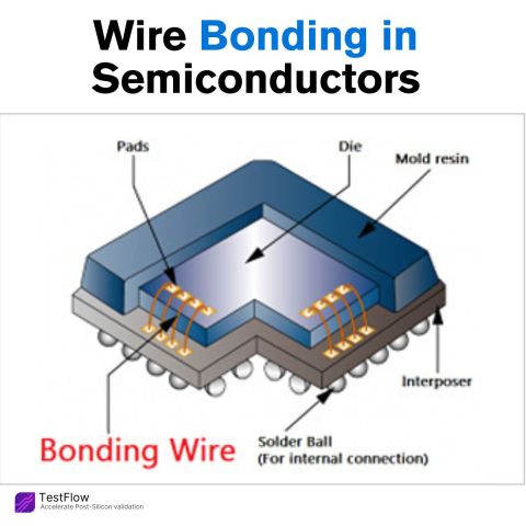
Wire bonding is the process of creating electrical connections between a semiconductor die and its package using ultrathin metallic wires. These microscopic cables—typically made of gold, aluminum, or copper—form the critical pathway for signals, power, and ground connections.
Key Components
- • Bond Wires: Ultra-fine metal wires (15-75 μm diameter)
- • Bond Pads: Metal contact areas on the chip
- • Lead Frame/Substrate: Package connection points
- • Interposer: Intermediate connection layer
- • Encapsulation: Protective molding compound
Wire Materials
- • Gold: Excellent conductivity, corrosion resistance
- • Aluminum: Cost-effective, good for high-volume
- • Copper: Superior electrical performance
- • Silver: Specialized high-frequency applications
- • Palladium-coated copper: Balance of cost and performance
Wire Bonding Process Flow
Die Attachment
Secure chip to package substrate
Wire Bonding
Connect die pads to package leads
Testing
Verify electrical connectivity
Encapsulation
Protect with molding compound
Wire Bonding Technologies
Ball Bonding (Gold Wire)
Process
- • Electric flame-off creates gold ball
- • Ball bonds to chip pad under pressure/heat
- • Wire extends to package lead frame
- • Stitch bond completes connection
- • Wire tail cut and process repeats
Advantages
- • Excellent reliability and corrosion resistance
- • Mature, well-understood process
- • Good for fine-pitch applications
- • Superior bond strength
- • Wide process window
Wedge Bonding (Aluminum Wire)
Process
- • Ultrasonic energy welds wire to pad
- • Wedge tool deforms wire for bonding
- • No ball formation required
- • Direct wire-to-pad contact
- • Suitable for aluminum metallization
Benefits
- • Lower material costs than gold
- • Good for high-volume production
- • Compatible with aluminum chip pads
- • Established automotive qualification
- • Suitable for power applications
Copper Wire Bonding
Technical Advantages
- • Superior electrical conductivity
- • Lower resistance than gold
- • Better thermal conductivity
- • Reduced electromigration
- • Cost-effective alternative to gold
Challenges
- • Oxidation sensitivity
- • Requires protective atmosphere
- • More complex bonding process
- • Tool wear considerations
- • Surface preparation critical
Understanding Package Architecture
From Silicon to System
Think of the die as a powerful workstation inside a sealed lab. Wire bonds are the power and data cables running through the walls—without them, the lab is isolated and useless.
Die & Bond Pads
The silicon chip with metal contact areas around its perimeter
- • Aluminum or copper metallization
- • Typically 50-100 μm square
- • Passivation layer protection
Wire Bonds
Ultrathin wires creating electrical pathways
- • 15-75 μm diameter
- • Gold, aluminum, or copper
- • Loop height: 50-200 μm
Package Substrate
The foundation connecting to external pins
- • Lead frame or organic substrate
- • Solder balls or pins
- • Thermal and electrical paths
Package Types Using Wire Bonding
Traditional Packages
- • QFP (Quad Flat Package)
- • QFN (Quad Flat No-lead)
- • SOIC (Small Outline IC)
- • TSSOP (Thin Shrink Small Outline)
- • DIP (Dual In-line Package)
Advanced Packages
- • BGA (Ball Grid Array)
- • CSP (Chip Scale Package)
- • MCM (Multi-Chip Module)
- • SiP (System in Package)
- • Power modules
Wire Bonding vs. Advanced Alternatives
Comparison Matrix
| Technology | Cost | Performance | Density | Complexity |
|---|---|---|---|---|
| Wire Bonding | Low | Good | Medium | Low |
| Flip Chip | Medium | Excellent | High | Medium |
| Through Silicon Via | High | Excellent | Very High | High |
| Hybrid Bonding | Very High | Superior | Ultra High | Very High |
Wire Bonding Strengths
- • Lowest cost and complexity
- • Mature, reliable technology
- • Wide supplier ecosystem
- • Excellent for cost-sensitive applications
- • Good for low-to-medium I/O count
- • Established qualification standards
- • Flexible design rules
Limitations
- • Limited I/O density
- • Longer electrical paths
- • Inductance and parasitics
- • Package height constraints
- • Speed limitations for high-frequency
- • Wire sweep in molding
- • Thermal performance constraints
Market Dominance and Applications
Why Wire Bonding Still Rules
Despite advances in flip-chip and other interconnect technologies, wire bonding remains the most common method in OSAT (Outsourced Semiconductor Assembly and Test) because it's simple, reliable, and cost-effective.
Of packaged ICs use wire bonding
Annual wire bonding equipment market
Of continuous technology evolution
Key Application Areas
Consumer Electronics
- • Microcontrollers and processors
- • Memory devices (DRAM, Flash)
- • Analog and mixed-signal ICs
- • Power management ICs
- • Sensors and MEMS devices
Industrial & Automotive
- • Automotive ECUs and sensors
- • Industrial control systems
- • Power electronics modules
- • RF and wireless modules
- • Medical device electronics
Future Evolution
Technology Improvements
- • Finer wire diameters (sub-15 μm)
- • Advanced wire materials
- • Improved bonding accuracy
- • Higher throughput equipment
- • Better process monitoring
Hybrid Approaches
- • Wire bonding + flip chip combination
- • Multi-tier wire bonding
- • Integration with advanced packaging
- • Specialized high-frequency designs
- • AI-optimized bonding patterns
Testing and Validation Challenges
Wire Bond Reliability Testing
Wire bonding creates thousands of microscopic connections that must work reliably for years. Testing these connections requires specialized techniques and equipment to ensure long-term reliability.
Critical Test Parameters
- • Bond strength (pull and shear tests)
- • Electrical continuity and resistance
- • Wire loop profile and height
- • Bond placement accuracy
- • Intermetallic formation
- • Thermal cycling performance
Reliability Stress Tests
- • High temperature storage (HTS)
- • Temperature cycling (TC)
- • Highly accelerated stress test (HAST)
- • Mechanical shock and vibration
- • Electromigration testing
- • Corrosion resistance evaluation
TestFlow for Wire Bond Validation
Modern wire bonding validation requires comprehensive testing of electrical performance, mechanical integrity, and long-term reliability. TestFlow's AI-powered platform automates complex wire bond characterization, reducing validation time while ensuring thorough coverage of all critical parameters.
Learn About Package TestingThe Enduring Legacy of Wire Bonding
Wire bonding represents one of the semiconductor industry's most successful technologies—a 50-year-old process that continues to evolve and adapt to modern requirements. While advanced packaging technologies capture headlines, wire bonding quietly enables the vast majority of electronic devices we use every day.
The technology's enduring success stems from its fundamental advantages: simplicity, cost-effectiveness, and reliability. As chips become more complex and manufacturing costs rise, these basic virtues become even more valuable. Wire bonding provides a proven, scalable solution that balances performance with practicality.
Looking ahead, wire bonding will continue to coexist with advanced packaging technologies, each serving different market segments and applications. The future belongs not to a single interconnect technology, but to the intelligent application of the right solution for each specific need—and wire bonding will remain a crucial part of that ecosystem.
Validate Your Packaging Technology
Whether you're using wire bonding, flip chip, or advanced packaging technologies, comprehensive validation ensures reliable connections and optimal performance. TestFlow's platform provides the testing capabilities you need for any packaging approach.