What's Inside an AI Chip? A Visual Breakdown of Modern AI Accelerators
AI isn't powered by just GPUs anymore. Modern AI chips are sophisticated systems-on-silicon, combining specialized processors, high-bandwidth memory, and custom interconnects. Discover the architectural innovations driving the AI revolution.
The AI revolution isn't just about algorithms and data—it's fundamentally about silicon. Modern AI chips are marvels of engineering that pack multiple specialized processing units, massive memory systems, and sophisticated interconnects onto single pieces of silicon. These aren't your traditional CPUs or even GPUs—they're purpose-built AI accelerators designed to handle the unique demands of machine learning workloads.
From Google's TPUs powering search to NVIDIA's H100s training the largest language models, AI chips represent the cutting edge of semiconductor design. Let's explore what makes these silicon brains tick.
Core AI Processing Units
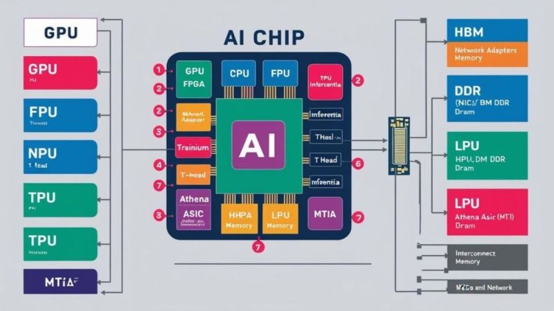
The AI Processing Ecosystem
Tensor Processing Units (TPUs)
Google's custom AI accelerators optimized for TensorFlow workloads
Neural Processing Units (NPUs)
Specialized processors for edge AI and mobile applications
Graphics Processing Units (GPUs)
Parallel processors adapted for AI training and inference
Field-Programmable Gate Arrays (FPUs)
Reconfigurable hardware for custom AI algorithms
AI-Specific Architecture Components
Inference vs Training Engines
Training Engines
Google TPU v4
Optimized for large-scale model training with BF16 precision
NVIDIA H100
Transformer engine with FP8 support for efficient training
Amazon Trainium
Custom training chips for AWS cloud workloads
Inference Engines
Amazon Inferentia
High-throughput, cost-effective inference acceleration
Intel Habana Goya
Specialized for computer vision and NLP inference
Qualcomm AI Engine
Edge AI processing for mobile and automotive
Custom AI ASICs
Meta MTIA
Meta's Training and Inference Accelerator for recommendation systems and NLP
Tesla Dojo
Supercomputer chip designed specifically for autonomous driving AI training
Alibaba T-Head
RISC-V based AI processors for cloud and edge applications
Memory Architecture: The AI Bottleneck
AI workloads are incredibly memory-intensive. Modern neural networks can have billions of parameters, requiring massive amounts of high-bandwidth memory to feed the processing units efficiently.
Memory Types in AI Chips:
High Bandwidth Memory (HBM)
Up to 3.2 TB/s bandwidth for GPU memory
GDDR6X
High-speed graphics memory for AI accelerators
LPDDR5
Low-power memory for edge AI applications
On-Chip SRAM
Ultra-fast cache for frequently accessed data
Memory Bandwidth Requirements:
Memory Hierarchy in AI Chips
Interconnect and Data Pipelines
On-Chip Interconnects
Network-on-Chip (NoC)
High-bandwidth, low-latency communication fabric connecting processing units
Ring Bus Architecture
Circular data paths for efficient core-to-core communication
Mesh Interconnect
Grid-based topology for scalable multi-core AI processors
High-Speed Interfaces
NVLink/NVSwitch
NVIDIA's proprietary high-bandwidth GPU-to-GPU communication
Infinity Fabric
AMD's scalable interconnect for CPU and GPU communication
PCIe 5.0/6.0
Industry-standard interfaces for AI accelerator cards
Data Flow Optimization
Dataflow Architectures
Minimize data movement by bringing computation to data
Systolic Arrays
Pipelined processing units for matrix operations
Sparsity Support
Skip zero-valued computations to improve efficiency
Leading AI Chip Examples
NVIDIA H100: The AI Training Powerhouse
Architecture
- • Hopper GPU architecture
- • 80 billion transistors (4nm)
- • 16,896 CUDA cores
- • 456 Tensor cores (4th gen)
Memory & Bandwidth
- • 80GB HBM3 memory
- • 3.35 TB/s memory bandwidth
- • 50MB L2 cache
- • 900 GB/s NVLink bandwidth
AI Performance
- • 4,000 TOPS (INT8 sparse)
- • 1,000 TFLOPS (BF16)
- • Transformer Engine
- • FP8 precision support
Google TPU v4: Custom AI Training
Design
- • Custom ASIC design
- • 7nm process node
- • Matrix multiplication units
- • Systolic array architecture
Memory System
- • 32GB HBM2 memory
- • 1.2 TB/s bandwidth
- • Vector processing units
- • Optical interconnects
Optimization
- • TensorFlow optimized
- • BF16 precision
- • 2.1x performance vs v3
- • Pod-scale deployment
Apple M2 Ultra: Edge AI Integration
SoC Design
- • 134 billion transistors
- • 5nm process (TSMC)
- • 24-core CPU
- • 76-core GPU
AI Acceleration
- • 32-core Neural Engine
- • 31.6 TOPS AI performance
- • 192GB unified memory
- • 800 GB/s memory bandwidth
Integration
- • Media engines
- • ProRes/ProRAW acceleration
- • Power efficiency focus
- • macOS optimization
AI Chip Validation Challenges
AI chips present unique validation challenges due to their complex architectures, massive parallelism, and diverse workload requirements. Traditional validation approaches often fall short.
Key Validation Challenges:
- • Massive parallel processing validation
- • Memory bandwidth and latency testing
- • Thermal management under AI workloads
- • Power consumption characterization
- • Accuracy verification across data types
- • Real-world AI workload simulation
- • Multi-chip system integration
Advanced Testing Approaches:
- • AI-driven test pattern generation
- • Synthetic neural network benchmarks
- • Real-time performance monitoring
- • Distributed testing across chip arrays
- • Machine learning model validation
- • Hardware-software co-validation
- • Continuous integration testing
TestFlow for AI Chip Validation
AI chips require specialized validation approaches that can handle their unique architectures and workloads. TestFlow's AI-powered platform provides comprehensive testing capabilities for modern AI accelerators, from single-chip validation to multi-chip system characterization.
Learn About AI Chip TestingThe Future of AI Chip Architecture
Emerging Trends
Neuromorphic Computing
Brain-inspired architectures that process information like biological neural networks
Photonic AI Accelerators
Using light instead of electrons for ultra-fast, low-power AI processing
Quantum-Classical Hybrid
Combining quantum processing units with classical AI accelerators
Processing-in-Memory
Eliminating data movement by performing computation directly in memory
Chiplet-Based AI Systems
Modular AI accelerators built from specialized chiplet components
Adaptive Architecture
AI chips that reconfigure themselves based on workload requirements
Market Projections
AI chip market size by 2030
Performance improvement target vs today
Energy efficiency improvement needed
The Silicon Brain Revolution
AI chips represent the cutting edge of semiconductor design, combining multiple specialized processing units, massive memory systems, and sophisticated interconnects to tackle the computational demands of artificial intelligence. These aren't just faster processors—they're fundamentally different architectures optimized for the parallel, data-intensive nature of AI workloads.
From Google's TPUs training language models to edge NPUs enabling real-time AI in smartphones, these silicon brains are reshaping what's possible in computing. As AI applications become more sophisticated and ubiquitous, the chips that power them will continue to evolve, pushing the boundaries of performance, efficiency, and capability.
Understanding AI chip architecture is crucial for anyone working in AI, semiconductor design, or system engineering. These components aren't just enabling today's AI revolution—they're laying the foundation for tomorrow's intelligent systems.
Validate Your AI Chips with Precision
AI chips require specialized validation to ensure they meet performance, accuracy, and reliability requirements. TestFlow's AI-powered platform provides comprehensive testing capabilities for modern AI accelerators and neural processing units.