Before any chip is packaged, shipped, or even separated from the wafer, it has to pass through the first critical checkpoint of validation: wafer-level testing, also known as wafer probe or wafer sort. This is the moment where we ask the fundamental question: does the silicon actually work?
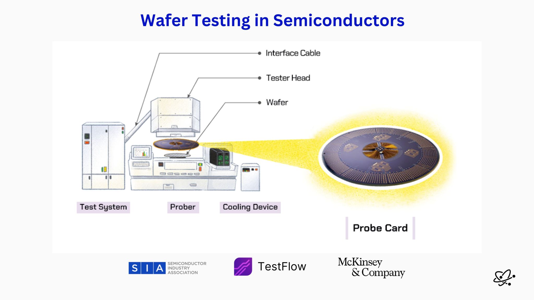
What You're Looking At: The Modern Probe Station
The image shows a modern probe station—a sophisticated machine that forms the backbone of semiconductor validation. This equipment enables engineers to test every individual die on a wafer while it's still intact, long before packaging or integration into final products.
A probe station is essentially a precision testing platform that combines mechanical positioning, electrical measurement, and environmental control into a single system capable of validating thousands of chips in a matter of hours.
Precision Positioning System
Modern probe stations use advanced positioning systems with sub-micron accuracy to align probe needles with tiny test pads on each die. This precision is critical as test pads can be as small as 50 micrometers—about half the width of a human hair.
Environmental Control
The station includes sophisticated thermal management systems that can heat or cool wafers to simulate operating conditions ranging from -40°C to +150°C, ensuring chips will function across their entire operating temperature range.
How Wafer Sort Testing Works
The wafer sort process is a carefully orchestrated sequence of mechanical positioning, electrical contact, and signal measurement. Here's how each component works together to validate silicon quality:
The Testing Process Step-by-Step
Wafer Loading and Alignment
The wafer is loaded onto a precision chuck that holds it perfectly flat. Advanced vision systems locate alignment marks on the wafer to establish a coordinate system for accurate die-to-die positioning.
Probe Card Contact
A probe card—containing hundreds of precisely positioned needles—makes contact with the test pads on each die. These needles must apply just enough force to ensure good electrical contact without damaging the delicate metal pads.
Electrical Testing
The tester applies electrical signals and measures responses to verify functionality. This includes DC parametric tests, AC timing tests, and functional pattern tests that exercise the chip's logic circuits.
Pass/Fail Decision
Based on test results, each die is classified as passing or failing. Failing dies are marked with ink dots, while passing dies proceed to the next manufacturing step.
System Components: The Architecture of Validation
A modern wafer sort system is made up of several major components, each engineered for precision and reliability:
Prober System
The mechanical heart of the system that precisely aligns and positions the wafer. Modern probers use air-bearing stages for vibration-free movement and can position wafers with nanometer-level accuracy.
Tester Head
Contains the electronics that generate test signals and measure chip responses. Advanced tester heads can apply thousands of different test patterns and measure responses with picosecond timing accuracy.
Thermal Management
Sophisticated heating and cooling systems that simulate real-world operating conditions. This ensures chips will function properly across their entire temperature specification range.
Interface System
High-speed cables and connectors that route signals between the tester and probe card. These must maintain signal integrity at frequencies up to several gigahertz for high-speed digital testing.

TestFlow: Next-Generation Validation Platform
Modern testing platforms like TestFlow are revolutionizing wafer sort testing with AI-powered analytics and automated test generation
Why Wafer Sort Testing Matters
Wafer sort testing represents the first opportunity to identify defects and separate good dies from bad ones. This early detection is crucial for several reasons:
Early Defect Detection
This is the first chance to spot critical defects including electrical shorts, opens, logic failures, and timing issues. Catching these problems early prevents wasted effort on packaging defective chips.
Yield Optimization
By identifying and marking bad dies early, wafer sort testing improves overall manufacturing yield. Only known-good dies proceed to expensive packaging and final test operations.
- Cost Reduction: Eliminating bad dies before packaging saves significant costs, as packaging can represent 30-50% of total manufacturing cost
- Quality Assurance: Ensures only functional chips proceed to final assembly, improving overall product reliability
- Process Feedback: Test results provide valuable feedback to fab engineers about process variations and potential improvements
- Supply Chain Efficiency: Prevents defective parts from entering the supply chain, reducing downstream quality issues
"The probe station is not just a testing machine—it's the gatekeeper of silicon quality. Before any burn-in, system-level testing, or packaging, this machine decides which dies live on and which are scrapped."
The Evolution of Wafer Sort Testing
As chips grow in complexity and manufacturing nodes shrink, probe stations are evolving rapidly to meet new challenges. Modern systems incorporate several advanced technologies:
AI-Based Analytics
Machine learning algorithms analyze test patterns to predict failures, optimize test sequences, and identify subtle defect signatures that traditional analysis might miss. This can improve defect detection rates by 15-25%.
Adaptive Testing
Modern systems can modify test parameters in real-time based on initial results, focusing additional testing on marginal dies while reducing test time for clearly passing or failing parts.
Supporting Advanced Architectures
Next-generation probe stations are being designed to handle emerging chip architectures:
- 2.5D/3D ICs: Advanced probe cards with multi-level contact capabilities for testing stacked and interposer-based designs
- Ultra-small nodes: Enhanced positioning accuracy and smaller probe needles for testing chips with increasingly tiny test pads
- High-speed interfaces: Support for testing multi-gigabit serial interfaces and advanced memory protocols
- Power management: Advanced power supply and measurement capabilities for testing complex power management circuits
The Future of Wafer Sort Testing
The semiconductor industry's relentless push toward smaller, faster, and more complex chips is driving continuous innovation in wafer sort testing. Key trends shaping the future include:
Parallel Testing: Future systems will test multiple dies simultaneously, dramatically reducing test time while maintaining accuracy. This is particularly important as wafer sizes increase and die counts per wafer grow.
In-Situ Characterization: Advanced probe stations will not just test for pass/fail but will also characterize each die's performance parameters, enabling better binning and yield optimization.
Predictive Maintenance: AI-powered systems will monitor probe station health and predict maintenance needs, reducing downtime and ensuring consistent test quality.
"It's where validation begins, silicon is sorted, and every chip earns its chance to move forward in the supply chain."
Conclusion: The Critical First Step
Wafer sort testing represents a critical inflection point in semiconductor manufacturing—the moment where theoretical chip designs meet the reality of silicon implementation. As the first comprehensive validation step, it serves as both a quality gate and a cost optimization tool.
The evolution of probe stations from simple electrical testers to sophisticated AI-powered validation platforms reflects the broader transformation of semiconductor manufacturing. As chips continue to grow in complexity and importance to our digital economy, the role of wafer sort testing will only become more critical.
For semiconductor manufacturers, investing in advanced wafer sort capabilities isn't just about improving current processes—it's about building the foundation for next-generation chip validation that will enable the continued advancement of semiconductor technology.
Revolutionize Your Wafer Sort Testing
TestFlow's advanced platform brings AI-powered analytics and automated test generation to wafer sort testing. Discover how leading semiconductor companies are reducing test time by 40% while improving defect detection rates.