In semiconductor manufacturing, yield is the fundamental metric that determines profitability and manufacturing efficiency. It represents the percentage of functional integrated circuit chips produced from a wafer compared to the total number of potential dies, directly impacting the cost-effectiveness of the entire fabrication process.
Understanding Semiconductor Yield: The Cookie Analogy
To understand semiconductor yield, imagine you're baking cookies. You place 24 cookie portions on a baking tray (representing a silicon wafer), but when they come out of the oven, only 20 cookies are perfectly shaped and properly baked (functional chips). Your yield would be 20/24 × 100% = 83.3%.
In semiconductor manufacturing, this analogy perfectly captures the essence of yield. A silicon wafer contains hundreds or thousands of individual chip locations (dies), but not all of them will function correctly after the complex fabrication process. The percentage of dies that pass all functional tests determines the yield of that wafer.
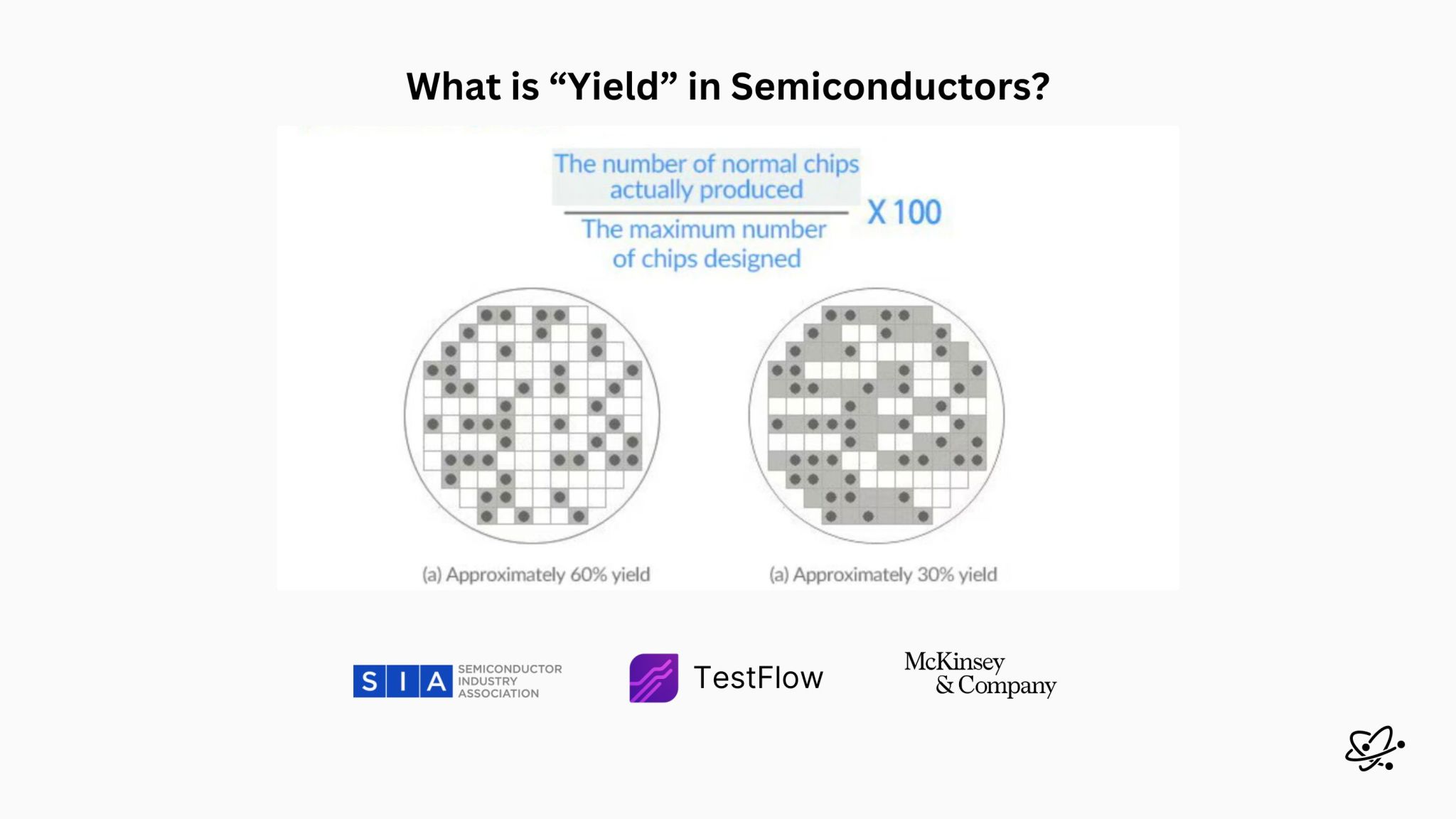
The Yield Formula
This simple formula drives billions of dollars in manufacturing decisions across the semiconductor industry
How Yield is Measured: The Wafer Sort Process
Determining yield requires a sophisticated testing process called "wafer sort" or "wafer probing." After the fabrication process is complete, each individual die on the wafer undergoes electrical testing to verify its functionality and performance against specifications.
Wafer Testing Process
Automated probe stations make electrical contact with each die on the wafer, running comprehensive test suites to verify functionality, performance parameters, and compliance with specifications.
- • Functional verification tests
- • Performance parameter validation
- • Power consumption measurements
- • Speed and timing verification
Pass/Fail Determination
Dies that meet all specification requirements are marked as functional, while those failing any test are marked as non-functional and will be discarded during the dicing process.
- • Binary pass/fail classification
- • Performance binning for different grades
- • Defect pattern analysis
- • Yield mapping across the wafer
Factors Affecting Semiconductor Yield
Multiple factors influence the total number of potential dies and the final yield percentage. Understanding these factors is crucial for optimizing manufacturing processes and improving profitability.
Wafer and Die Geometry
The physical characteristics of the wafer and individual dies directly impact the maximum number of dies that can fit on a wafer.
- Wafer Size: Larger wafers (300mm vs 200mm) can accommodate more dies, improving economies of scale
- Die Size: Smaller dies mean more potential dies per wafer, but also potentially lower individual die performance
- Scribe Lines: The spacing between dies where the wafer is cut affects total die count
Manufacturing Process Factors
The complexity and maturity of the manufacturing process significantly impact yield rates.
- Process Node Maturity: Newer, smaller nodes typically have lower initial yields
- Defect Density: Particles, contamination, and process variations can cause functional failures
- Design Complexity: More complex circuits have higher probability of defects
The Yield Journey: From New Node to Commercial Viability
Understanding the typical yield progression for new semiconductor nodes provides insight into the challenges and economics of advanced manufacturing.
Yield Progression Timeline
How semiconductor yields typically improve from initial development to high-volume manufacturing
Initial Development (0-20% Yield)
When a new process node is first developed, yields are extremely low as engineers work to understand and optimize the manufacturing process. Most dies fail due to process variations and defects.
Process Optimization (20-50% Yield)
Through systematic process improvements, defect reduction, and design-for-manufacturability enhancements, yields gradually improve. This phase can take 12-24 months.
Early Production (50-70% Yield)
Limited production begins for premium products where customers are willing to pay higher prices. Continued process refinement and learning from production data drive improvements.
Commercial Viability (70-90% Yield)
High-volume manufacturing becomes economically viable. At this stage, the process is mature enough to support mainstream products with competitive pricing.
Industry Leaders: TSMC vs Samsung Yield Competition
The competition between leading foundries often comes down to who can achieve higher yields faster on new process nodes. This directly impacts their ability to win customer designs and generate profits.
TSMC's Yield Leadership
Taiwan Semiconductor Manufacturing Company (TSMC) has consistently demonstrated superior yield performance across multiple process nodes, contributing to their market leadership position.
Samsung's Aggressive Progress
Samsung Foundry has been investing heavily in yield improvement, showing significant progress on advanced nodes, particularly their 2nm process development.
"Recent reports from February 2025 indicate that Samsung's initial yield for its 2nm process used in the Exynos 2600 was around 30% in trial production. While still behind TSMC's estimated 60% for their 2nm process, this represents significant improvement for Samsung and demonstrates the rapid pace of yield optimization in advanced nodes."
Node-Specific Yield Variations: Size and Complexity Matter
It's crucial to understand that yield figures vary significantly depending on the specific design and complexity of the chip being produced. A large, complex server CPU will typically have lower yield than a smaller, simpler mobile application processor on the same process node.
| Chip Type | Typical Die Size | Expected Yield Range | Complexity Factor |
|---|---|---|---|
| Mobile Application Processor | 50-100 mm² | 80-90% | Medium |
| GPU (High-end) | 400-800 mm² | 60-75% | High |
| Server CPU | 300-600 mm² | 50-70% | Very High |
| AI Accelerator | 500-900 mm² | 40-60% | Extremely High |
The Economics of Yield: Why Every Percentage Point Matters
Understanding the economic impact of yield improvements helps explain why semiconductor companies invest billions of dollars in yield optimization. Small improvements in yield can translate to massive cost savings and competitive advantages.
Yield Impact Example: High-End GPU
Consider a high-end GPU with the following characteristics:
Manufacturing Parameters
- • Die size: 600 mm²
- • Dies per wafer: ~100
- • Wafer cost: $15,000
- • Selling price: $1,200
Yield Impact Analysis
- • 50% yield: 50 good dies, $300 cost per die
- • 60% yield: 60 good dies, $250 cost per die
- • 70% yield: 70 good dies, $214 cost per die
- • 10% yield improvement = $36 cost reduction per die
For a company producing 1 million GPUs annually, a 10% yield improvement saves $36 million in manufacturing costs
Beyond Fabrication: Post-Silicon Validation and TestFlow
While yield optimization focuses on the fabrication process, ensuring that functional dies actually work correctly in real-world applications requires comprehensive post-silicon validation. This is where advanced testing and validation platforms become crucial.
At Atoms, we're addressing the critical post-fabrication challenges that impact overall silicon reliability and time-to-market. Even chips that pass wafer sort testing may have subtle issues that only emerge during comprehensive system-level validation.
TestFlow: Accelerating Post-Silicon Validation

Our platform, TestFlow, helps chip teams accelerate lab testing, uncover hidden bugs faster, and improve chip bring-up efficiency. While yield optimization ensures more dies pass initial fabrication, TestFlow ensures those dies work reliably in real-world applications.
By combining fabrication yield optimization with advanced post-silicon validation, semiconductor companies can maximize both the quantity and quality of functional chips reaching the market, ensuring optimal return on their substantial manufacturing investments.
The Future of Yield Optimization
As semiconductor manufacturing continues to push the boundaries of physics with smaller nodes and more complex designs, yield optimization becomes increasingly challenging and critical. Advanced analytics, machine learning, and AI-driven process control are becoming essential tools for maintaining and improving yields.
- AI-Driven Process Control: Machine learning algorithms analyze vast amounts of manufacturing data to predict and prevent yield-limiting defects
- Advanced Metrology: More sophisticated measurement and inspection tools enable earlier detection of process variations
- Design-Process Co-optimization: Closer collaboration between design and manufacturing teams to optimize both design and process for higher yields
- Predictive Maintenance: Equipment health monitoring and predictive maintenance to minimize process variations
Conclusion: Yield as the Foundation of Semiconductor Economics
Semiconductor yield represents far more than a simple manufacturing metric—it's the foundation upon which the entire economics of chip production rests. From the initial cookie analogy to the complex realities of advanced node manufacturing, yield directly determines whether new technologies can be commercially viable.
As we've seen, industry leaders like TSMC maintain their competitive advantage through superior yield performance, while companies like Samsung invest heavily to close the gap. The progression from initial development yields below 50% to commercial viability above 70% requires years of investment and optimization.
Looking forward, the combination of advanced fabrication yield optimization and comprehensive post-silicon validation will be essential for maximizing the value of semiconductor manufacturing investments. Companies that excel in both areas will be best positioned to deliver the reliable, high-performance chips that power our digital future.
Optimize Your Post-Silicon Validation
While you optimize fabrication yields, don't let post-silicon validation become your bottleneck. Learn how TestFlow can help you accelerate testing, uncover hidden issues, and improve chip bring-up efficiency.