Major Players in Semiconductor Packaging Ecosystem: The Unsung Heroes of Chip Assembly
Behind every finished chip lies a complex ecosystem of packaging specialists, material innovators, and precision equipment makers. Discover the major players shaping this critical supply chain that connects silicon to the real world.
While chip design and manufacturing capture headlines, semiconductor packaging represents one of the industry's most critical—yet underappreciated—segments. This ecosystem transforms bare silicon dies into finished products that can survive the real world, connecting microscopic circuits to the macro-scale systems we use every day.
From OSATs handling billions of chips annually to specialized material suppliers enabling advanced packaging innovations, this network of companies ensures that cutting-edge silicon reaches consumers reliably and cost-effectively. As chips become more advanced, packaging has evolved from a commodity service to a true competitive advantage.
OSAT Leaders: The Volume Champions
Outsourced Semiconductor Assembly & Test Giants
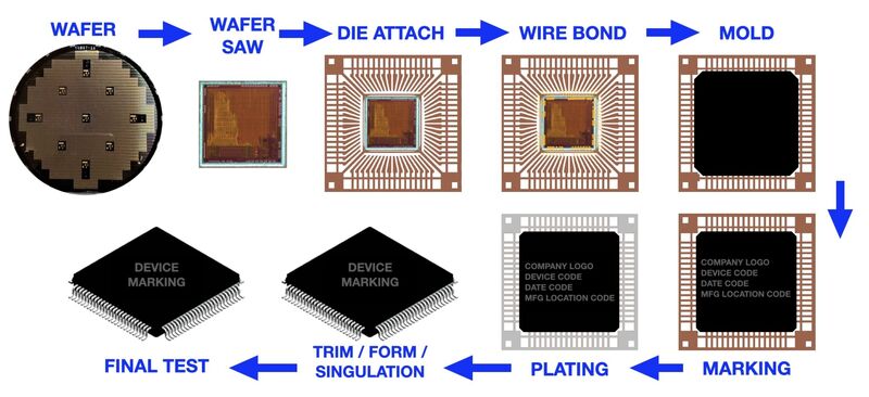
OSATs handle high-volume assembly, advanced packaging, and final testing at scale for the world's biggest fabless brands. These companies process billions of chips annually with precision and reliability.
ASE Group
World's Largest OSAT
Services
- • IC packaging and testing
- • System-in-Package (SiP)
- • Electronic manufacturing
- • Automotive electronics
Capabilities
- • Advanced packaging (2.5D/3D)
- • High-volume production
- • Global facility network
- • Automotive qualification
Key Customers
- • Apple (iPhone packaging)
- • Qualcomm
- • MediaTek
- • Automotive OEMs
Amkor Technology
Advanced Packaging Leader
Specialization
- • Advanced packaging focus
- • Flip chip technology
- • Wafer-level packaging
- • System-in-Package
Innovation
- • Fan-out wafer-level packaging
- • Embedded die technology
- • High-density interconnects
- • Thermal management solutions
Markets
- • Mobile and consumer
- • Automotive electronics
- • Communications infrastructure
- • Computing and storage
JCET Group
Chinese OSAT Leader
Strengths
- • Cost-competitive operations
- • Rapid capacity expansion
- • Broad technology portfolio
- • Local China market access
Services
- • Traditional packaging
- • Advanced packaging
- • Testing services
- • System integration
Growth Areas
- • 5G infrastructure
- • Automotive electronics
- • IoT devices
- • Memory packaging
IDMs with In-House Packaging Capabilities
Vertical Integration Advantages
Intel, Samsung, and Texas Instruments invest heavily in their own packaging lines to secure quality control, capacity, and technology development. This vertical integration provides strategic advantages but requires massive capital investment.
Intel
- • Advanced packaging R&D leader
- • Foveros 3D technology
- • EMIB 2.5D integration
- • Co-EMIB hybrid packaging
- • Ponte Vecchio implementation
Samsung
- • Memory packaging expertise
- • HBM stacking technology
- • Mobile SoC packaging
- • I-Cube4 advanced packaging
- • Automotive qualification
Texas Instruments
- • Analog packaging optimization
- • Automotive-grade reliability
- • Power management packaging
- • Industrial applications focus
- • Long-term supply commitment
In-House vs Outsourced Strategies
In-House Benefits
- • Complete technology control
- • Faster innovation cycles
- • IP protection and security
- • Custom process optimization
- • Integrated quality systems
OSAT Advantages
- • Lower capital requirements
- • Economies of scale
- • Specialized expertise
- • Flexible capacity
- • Risk sharing
Equipment Providers: Precision at Scale
Backend Equipment Leaders
Kulicke & Soffa, ASM Pacific, and Tokyo Electron build the wire bonders, flip-chip placers, and advanced fan-out tools that power the backend of semiconductor manufacturing.
Kulicke & Soffa
- • Wire bonding equipment leader
- • Advanced packaging tools
- • Copper and gold wire bonding
- • High-speed, high-accuracy systems
- • LED packaging equipment
ASM Pacific
- • Die bonding and packaging
- • SMT placement equipment
- • Advanced packaging solutions
- • Automotive electronics focus
- • LED and optoelectronics
Tokyo Electron
- • Wafer-level packaging
- • Advanced lithography
- • Coating and developing
- • Thermal processing
- • Clean technology solutions
Advanced Packaging Equipment
Wire Bonding Equipment
- • Ball bonding systems for gold wire
- • Wedge bonding for aluminum wire
- • Copper wire bonding solutions
- • High-speed automated systems
- • Vision systems for precision placement
Advanced Assembly Tools
- • Flip-chip placement and reflow
- • Wafer-level packaging tools
- • Fan-out packaging equipment
- • 3D stacking and TSV processing
- • Hybrid bonding systems
Substrate and Material Suppliers: The Foundation
Critical Material Ecosystem
Ibiden, Unimicron, Shinko Electric, and Ajinomoto provide critical organic substrates and packaging materials that connect silicon to the outside world. These materials must meet stringent electrical, thermal, and mechanical requirements.
Substrate Leaders
Ibiden
High-end IC substrates, automotive focus
Unimicron
PCB and IC substrate manufacturing
Shinko Electric
Advanced IC substrates and packages
AT&S
European substrate and PCB leader
Material Innovations
Ajinomoto Build-up Film
Advanced dielectric materials for fine-pitch routing
Dow Chemical
Molding compounds and adhesives
Henkel
Die attach materials and underfills
Namics
Specialty packaging materials
Advanced Material Requirements
Electrical Properties
- • Low dielectric constant
- • Controlled impedance
- • Signal integrity preservation
- • EMI shielding capabilities
Thermal Management
- • High thermal conductivity
- • Low coefficient of thermal expansion
- • Heat spreading capabilities
- • Thermal interface materials
Reliability
- • Moisture resistance
- • Mechanical durability
- • Chemical compatibility
- • Long-term stability
Market Dynamics and Future Trends
Packaging Market Evolution
As chips become more advanced, packaging has moved from a commodity to a true competitive advantage. Innovations in 2.5D, 3D, fan-out, and chiplet integration are only as strong as the supply chain behind them.
Market Growth Drivers
- • AI accelerator packaging demands
- • 5G infrastructure requirements
- • Automotive electronics growth
- • IoT device miniaturization
- • Advanced packaging adoption
- • Chiplet architecture trends
Technology Trends
- • Fan-out wafer-level packaging (FOWLP)
- • System-in-Package (SiP) integration
- • Heterogeneous integration
- • Embedded die technologies
- • Advanced thermal solutions
- • AI-optimized packaging
Market Size and Projections
Global OSAT market (2024)
Annual growth rate (CAGR)
Projected market size by 2030
Packaging Validation and Quality Assurance
Critical Quality Parameters
Semiconductor packaging must meet stringent reliability requirements across diverse operating conditions. Quality assurance spans from individual component testing to complete system validation.
Key Test Parameters
- • Electrical continuity and resistance
- • Mechanical bond strength
- • Thermal cycling performance
- • Moisture sensitivity levels
- • Package warpage and stress
- • Solder joint reliability
Reliability Standards
- • JEDEC qualification standards
- • Automotive AEC-Q100/Q200
- • Industrial temperature ranges
- • Military and aerospace specs
- • Consumer electronics requirements
- • Medical device standards
TestFlow for Packaging Validation
Modern packaging technologies require comprehensive validation that spans from individual component testing to complete system characterization. TestFlow's AI-powered platform automates complex packaging validation workflows, ensuring reliability across all operating conditions.
Learn About Packaging TestingThe Future of Semiconductor Packaging
Emerging Technologies and Trends
Next-Generation Packaging
- • Hybrid bonding for ultra-fine pitch
- • Glass substrates for large panels
- • Photonic packaging integration
- • Quantum device packaging
- • Flexible and stretchable packages
Industry Evolution
- • Packaging becoming system-level design
- • Closer collaboration with chip designers
- • AI-driven packaging optimization
- • Sustainability and environmental focus
- • Geopolitical supply chain diversification
Strategic Implications
Packaging becoming part of chip design
New performance vectors beyond scaling
Packaging as competitive differentiation
The Unsung Heroes of Silicon Success
The semiconductor packaging ecosystem represents one of the industry's most critical yet underappreciated segments. From OSATs processing billions of chips annually to material suppliers enabling advanced packaging innovations, these companies ensure that cutting-edge silicon reaches consumers reliably and cost-effectively.
As chips become more complex and performance demands increase, packaging has evolved from a commodity service to a strategic differentiator. The companies that master advanced packaging technologies—2.5D integration, 3D stacking, and heterogeneous integration—will enable the next generation of electronic systems.
The future belongs to those who understand that great chips require great packaging. In an industry where every connection matters and every nanometer counts, the packaging ecosystem provides the critical bridge between silicon innovation and real-world application.
Optimize Your Packaging Validation Process
Advanced packaging technologies require sophisticated validation to ensure reliability and performance. TestFlow's AI-powered platform provides comprehensive testing capabilities for all packaging approaches, from traditional wire bonding to cutting-edge 3D integration.