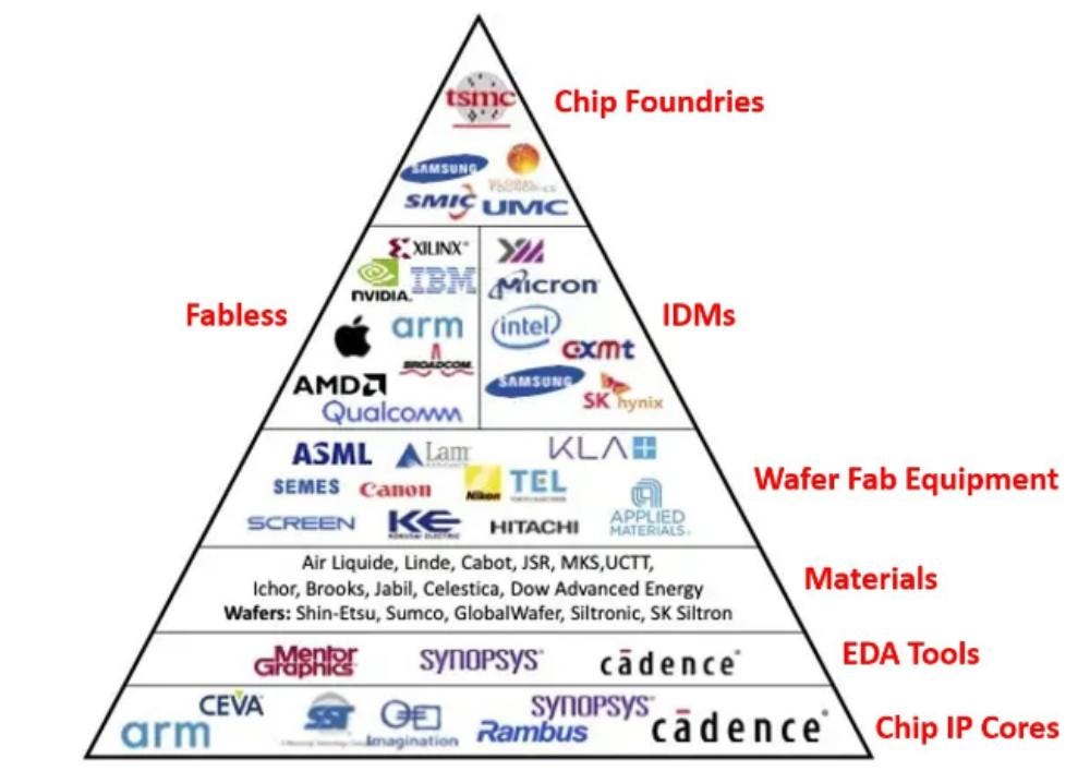
The semiconductor industry is a complex ecosystem where specialized companies collaborate to create the chips powering our modern world. From intellectual property cores to final assembly and testing, understanding these eight key player types reveals how the $600+ billion semiconductor industry operates.
The semiconductor industry's complexity stems from the incredible specialization required to create modern chips. No single company can efficiently handle every aspect of chip development and manufacturing. Instead, the industry has evolved into a sophisticated ecosystem where each player type focuses on their core competencies.
1. Chip Intellectual Property (IP) Cores
These companies design and license specific components or blocks of a chip, such as processors, memory controllers, or communication interfaces. They're the architects of fundamental chip building blocks.
What IP Core Companies Do
IP core companies develop reusable circuit designs that other companies can license and integrate into their chips. This enables faster development and reduces costs by leveraging proven designs.
Key Examples:
- • Arm: CPU cores (Cortex series)
- • Imagination Technologies: GPU cores
- • Cadence Design Systems: Interface IP
- • Synopsys: Memory and processor IP
Core IP Types:
- • Processor cores (CPU, GPU, DSP)
- • Memory controllers and interfaces
- • Communication protocols (USB, PCIe)
- • Security and encryption modules
"Arm's CPU designs power over 95% of smartphones worldwide, demonstrating how IP licensing enables global semiconductor innovation without every company needing to design processors from scratch."
2. Electronic Design Automation (EDA) Tools
EDA companies provide the software tools that chip designers use to create, simulate, and verify chip designs. They're the digital infrastructure enabling modern semiconductor design.
EDA Tool Categories
- • Design Entry: Circuit schematic capture
- • Simulation: Functional and timing verification
- • Synthesis: Converting designs to physical layouts
- • Place & Route: Physical chip layout optimization
- • Verification: Design rule checking and validation
Major EDA Companies
- • Synopsys: Leading design and verification tools
- • Cadence: Comprehensive EDA suite
- • Siemens EDA: (formerly Mentor Graphics)
- • Ansys: Simulation and analysis tools
- • Keysight: Test and measurement integration
3. Specialized Materials
These companies supply the ultra-pure chemicals, gases, and materials essential for semiconductor manufacturing. They enable the precise chemistry required for chip fabrication.
Critical Materials and Suppliers
Electronic Gases:
- • Air Products: Ultra-pure gases
- • Linde: Specialty gas mixtures
- • Matheson: Process gases
Chemicals & Materials:
- • DuPont: Photoresists and chemicals
- • Shin-Etsu: Silicon wafers
- • JSR: Advanced materials
These materials must meet extraordinary purity standards—often 99.9999% or higher—because even tiny impurities can cause chip defects.
4. Wafer Fab Equipment (WFE)
WFE companies manufacture the complex machines and equipment used in semiconductor fabrication plants. They create the tools that transform raw silicon into sophisticated integrated circuits.
| Equipment Type | Leading Companies | Key Function |
|---|---|---|
| Lithography | ASML, Canon, Nikon | Pattern printing on wafers |
| Etching | Lam Research, Applied Materials | Material removal and patterning |
| Deposition | Applied Materials, Tokyo Electron | Thin film layer creation |
| Metrology | KLA, Applied Materials | Measurement and inspection |
5. "Fabless" Chip Companies
Fabless companies focus entirely on chip design and marketing, outsourcing all manufacturing to foundries. This model enables rapid innovation without massive capital investments in fabrication facilities.
Fabless Advantages
- • Lower capital requirements
- • Focus on design innovation
- • Faster time-to-market
- • Access to latest process nodes
- • Reduced operational complexity
Leading Fabless Companies
- • Qualcomm: Mobile processors and modems
- • NVIDIA: GPUs and AI accelerators
- • MediaTek: Mobile and connectivity chips
- • Broadcom: Communication and infrastructure
- • AMD: CPUs and GPUs
"The fabless model has democratized chip innovation, allowing companies to focus on design excellence while leveraging the manufacturing expertise of specialized foundries."
6. Integrated Device Manufacturers (IDMs)
IDMs handle the complete chip lifecycle—from design through manufacturing to sales. They maintain control over their entire supply chain but require massive capital investments.
IDM Model Characteristics
Advantages:
- • Complete supply chain control
- • Process optimization for specific products
- • Better margins on high-volume products
- • Proprietary process technologies
Major IDMs:
- • Intel: Processors and data center chips
- • Samsung: Memory and mobile processors
- • SK Hynix: Memory solutions
- • Micron: Memory and storage
7. Chip Foundries
Foundries specialize in manufacturing chips for other companies, offering advanced fabrication processes without competing in chip design. They're the manufacturing backbone of the fabless ecosystem.
TSMC
Market leader with ~54% global foundry share
- • Leading-edge processes (3nm, 5nm)
- • Advanced packaging capabilities
- • Serves Apple, NVIDIA, AMD
Samsung Foundry
Second-largest foundry with ~17% market share
- • Competitive advanced nodes
- • Strong in memory integration
- • Serves Qualcomm, Google
GlobalFoundries
Third-largest with focus on specialty processes
- • Automotive and IoT focus
- • Mature node specialization
- • RF and analog expertise
8. Outsourced Semiconductor Assembly and Test (OSAT)
OSAT companies provide packaging, testing, and final assembly services for semiconductor chips. They transform bare dies into finished, tested products ready for market.
OSAT Services and Leaders
Assembly Services
Die attachment, wire bonding, and encapsulation to create packaged chips from bare dies.
Leaders: ASE Group, Amkor Technology, JCET
Testing Services
Comprehensive testing to ensure chips meet specifications before shipping to customers.
Leaders: Powertech Technology, ChipMOS, King Yuan Electronics
Advanced Packaging
System-in-package, 3D packaging, and other advanced solutions for complex applications.
Leaders: ASE Group, Amkor, STATS ChipPAC
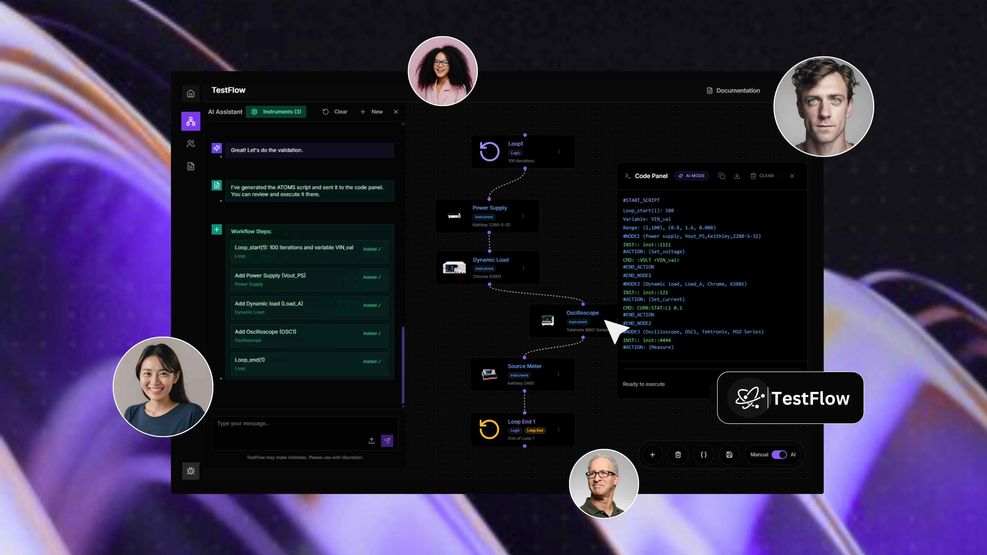
TestFlow: Enabling Ecosystem Collaboration
TestFlow supports testing and validation across the entire semiconductor ecosystem, from fabless design to OSAT final testing
How the Ecosystem Works Together
The semiconductor ecosystem's strength lies in its interconnectedness. Here's how these player types collaborate to create modern chips:
Typical Chip Development Flow
TestFlow's Role in the Ecosystem
TestFlow supports multiple player types across the semiconductor ecosystem, providing testing and validation solutions that enable collaboration and quality assurance:
For Fabless Companies
- • Design verification and validation
- • Pre-silicon testing strategies
- • Foundry collaboration tools
- • Quality assurance workflows
For Foundries & OSATs
- • Wafer-level testing automation
- • Yield optimization analytics
- • Final test validation
- • Customer collaboration platforms
Industry Trends Shaping the Ecosystem
Several trends are reshaping how these ecosystem players interact and collaborate:
- Chiplet Architecture: Enabling new collaboration models between IP providers and integrators
- AI/ML Integration: Driving demand for specialized testing and validation capabilities
- Advanced Packaging: Requiring closer collaboration between foundries and OSATs
- Sustainability Focus: Driving efficiency improvements across all ecosystem players
"The semiconductor ecosystem's complexity is also its strength—specialized companies working together can achieve what no single company could accomplish alone."
Conclusion: A Symphony of Specialization
The semiconductor ecosystem represents one of the most sophisticated examples of industrial specialization in human history. Each of the eight player types contributes essential capabilities:
• IP Cores: Reusable circuit designs
• EDA Tools: Design and verification software
• Materials: Ultra-pure chemicals and gases
• WFE: Manufacturing equipment
• Fabless: Innovation-focused design
• IDMs: Integrated manufacturing control
• Foundries: Specialized manufacturing
• OSATs: Assembly and testing
Understanding this ecosystem is crucial for anyone working in semiconductors, whether you're developing chips, providing services, or enabling collaboration between these specialized players. The industry's continued innovation depends on the seamless interaction of all eight player types.
Enable Ecosystem Collaboration with TestFlow
TestFlow bridges the gap between ecosystem players, providing comprehensive testing and validation solutions that enable seamless collaboration from design to delivery. Join the companies building the future of semiconductors.