Most Important EDA Tools: From Design to Market Success
Every semiconductor device starts with EDA tools, but the journey doesn't end at tape-out. Discover the critical EDA tools powering chip design and why post-silicon validation is becoming the final frontier for market success.
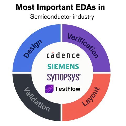
Every semiconductor device in the world—from the simplest sensor to the most advanced AI accelerator—begins its journey in Electronic Design Automation (EDA) tools. These software platforms enable engineers to design, simulate, and verify chips containing billions of transistors, transforming abstract concepts into manufacturable silicon.
But the story doesn't end at tape-out. As chip complexity explodes and validation becomes increasingly critical, a new category of tools is emerging to bridge the gap between EDA design and market success: AI-powered post-silicon validation platforms that ensure chips work perfectly in the real world.
Essential EDA Tools by Design Stage
Logic Synthesis: Synopsys Design Compiler
Market Position
- • Industry standard for 30+ years
- • Used in 90%+ of digital designs
- • Synopsys flagship product
- • Continuous innovation leader
Capabilities
- • RTL to gate-level transformation
- • Technology mapping optimization
- • Timing and area optimization
- • Power reduction techniques
Advanced Features
- • AI-driven optimization
- • Multi-voltage domain support
- • Advanced node compatibility
- • Clock gating automation
Physical Design: Cadence Innovus
Core Functions
- • Floorplanning and placement
- • Clock tree synthesis
- • Routing optimization
- • Timing closure automation
Advanced Capabilities
- • Machine learning optimization
- • Multi-corner analysis
- • Advanced node support
- • Power optimization
Market Impact
- • Leading P&R solution
- • Complex SoC enablement
- • Foundry collaboration
- • Advanced packaging support
Analog Design: Cadence Virtuoso
Design Environment
- • Custom circuit design
- • Schematic capture
- • Layout and verification
- • Parasitic extraction
Simulation
- • SPICE-accurate simulation
- • Monte Carlo analysis
- • Process variation modeling
- • RF and mixed-signal support
Applications
- • RF circuit design
- • Power management ICs
- • High-speed interfaces
- • Sensor interface circuits
Critical Verification and Validation Tools
Pre-Silicon Verification Leaders
Synopsys VCS
- • High-performance RTL simulation
- • SystemVerilog and UVM support
- • Debug and coverage analysis
- • Acceleration and emulation
Siemens QuestaSim
- • Mixed-signal simulation
- • Advanced debug capabilities
- • Verification methodology support
- • Formal verification integration
Timing and Power Analysis
Synopsys PrimeTime
- • Static timing analysis gold standard
- • Advanced node timing closure
- • Multi-corner optimization
- • Clock domain crossing analysis
Cadence Voltus
- • Power integrity analysis
- • IR drop analysis
- • Electromigration checking
- • Power grid optimization
The Missing Link: Post-Silicon Validation
Where EDA Ends and Reality Begins
While EDA tools handle pre-silicon design and simulation, there's a critical gap between tape-out and market success: post-silicon validation. This is where chips must prove they work correctly in real-world conditions, not just in simulation.
Post-Silicon Challenges
- • Silicon doesn't match simulation perfectly
- • Process variations affect performance
- • Real-world operating conditions
- • Complex system interactions
- • Time pressure for market launch
- • Debug access limitations
Validation Requirements
- • Functional verification on silicon
- • Performance characterization
- • Power and thermal validation
- • Reliability and stress testing
- • Software integration validation
- • Production test development
The Validation Crisis
Of chip development time now spent on validation
Validation costs for 2nm chips
Typical post-silicon validation timeline
TestFlow: Bridging EDA and Market Success
AI-Powered Post-Silicon Validation
TestFlow by ATOMS represents a new category in the EDA ecosystem—AI-powered post-silicon validation that automates lab workflows, integrates with instruments, and shortens debug cycles. While EDA tools handle design, TestFlow ensures market readiness.
Core Capabilities
- • Automated test sequence generation
- • Instrument integration and control
- • Real-time data capture and analysis
- • AI-driven pattern recognition
- • Automated report generation
Workflow Integration
- • Datasheet-driven test creation
- • Lab equipment orchestration
- • Continuous integration support
- • Version control integration
- • Collaboration tools
AI Advantages
- • Intelligent test optimization
- • Anomaly detection
- • Root cause analysis
- • Predictive failure analysis
- • Learning from validation data
The Complete Design-to-Market Flow
EDA Design Phase
Synopsys, Cadence, Siemens tools for RTL design, synthesis, and implementation
Manufacturing
TSMC, Samsung foundries fabricate the silicon using advanced processes
TestFlow Validation
AI-powered post-silicon validation ensures chips work perfectly in real conditions
Market Success
Validated chips ship to customers with confidence in performance and reliability
EDA Market Evolution and Future Trends
Market Size and Growth
Current Market (2024)
Growth Drivers
- • AI chip design complexity
- • Advanced node requirements
- • System-level design needs
- • Automotive electronics growth
- • Cloud-based EDA adoption
- • Post-silicon validation demand
AI Integration in EDA
Design Optimization
- • ML-driven synthesis optimization
- • AI-assisted place and route
- • Automated design space exploration
- • Intelligent constraint generation
Verification Acceleration
- • AI-generated test patterns
- • Smart coverage analysis
- • Automated debug assistance
- • Regression test optimization
Post-Silicon Innovation
- • Intelligent test automation
- • Anomaly detection systems
- • Predictive failure analysis
- • Automated root cause analysis
Future EDA Ecosystem
EDA market size by 2030
Next-generation tools built AI-first
Shift to cloud-native EDA platforms
Industry Impact: Enabling the Impossible
EDA's Role in Semiconductor Success
EDA tools don't just enable chip design—they determine what's possible in semiconductor technology. Without sophisticated software, billion-transistor chips would be impossible to design, verify, or manufacture reliably.
Industry Enablement
- • Makes complex chip design feasible
- • Reduces design time from years to months
- • Enables advanced node adoption
- • Facilitates design reuse and IP sharing
- • Supports global design collaboration
Innovation Acceleration
- • Rapid prototyping and iteration
- • Design space exploration
- • Automated optimization
- • Cross-domain integration
- • Continuous improvement cycles
The Complete Tool Ecosystem
Traditional EDA Strengths
- • Pre-silicon design and verification
- • Synthesis and implementation
- • Timing and power analysis
- • Physical design and layout
Post-Silicon Innovation
- • Real silicon validation and debug
- • Performance characterization
- • Production test automation
- • System-level validation
Measuring EDA and Validation Success
Key Performance Indicators
Design Efficiency Metrics
- • Time from concept to tape-out
- • First-pass silicon success rate
- • Design iterations required
- • Verification coverage achieved
- • Design team productivity
Validation Success Metrics
- • Post-silicon debug time
- • Time to market achievement
- • Validation coverage completeness
- • Field failure rates
- • Customer satisfaction scores
Industry Success Stories
Reduction in validation time with AI tools
First-pass success rate with modern EDA
Average time-to-market improvement
The Evolution of Chip Development
The EDA ecosystem has evolved from simple design tools to sophisticated platforms that enable the creation of the world's most complex devices. As chips become more advanced and time-to-market pressures intensify, the integration of design, manufacturing, and validation tools becomes increasingly critical.
The emergence of AI-powered validation platforms like TestFlow represents the next evolution in this ecosystem—bridging the gap between EDA design excellence and market success. While traditional EDA tools handle the complexity of design, these new platforms ensure that silicon performs flawlessly in the real world.
Success in modern semiconductor development requires mastery of the complete flow—from initial concept through design, manufacturing, validation, and market deployment. The companies that excel across this entire spectrum will define the future of semiconductor innovation.
Complete Your Design-to-Market Flow
While EDA tools handle design and synthesis, TestFlow completes the journey to market success. Our AI-powered platform ensures your chips work perfectly in real-world conditions, accelerating time-to-market with confidence.