Ever wondered how a chip is made? The journey from a bare silicon wafer to a powerful microchip is one of the most complex manufacturing processes on Earth, combining chemistry, physics, nanotechnology, and automation with almost zero room for error. Let's explore this fascinating step-by-step process that creates the foundation of our digital world.
The Marvel of Semiconductor Manufacturing
Semiconductor manufacturing represents one of humanity's greatest technical achievements. The process transforms simple silicon—the second most abundant element on Earth—into sophisticated computing devices capable of billions of calculations per second. This transformation requires hundreds of precisely controlled steps, each executed with atomic-level precision in some of the cleanest environments ever created.
To put this in perspective, modern semiconductor manufacturing operates at scales smaller than viruses. A typical transistor in today's advanced chips measures just a few nanometers—approximately 10,000 times smaller than the width of a human hair. Creating billions of these transistors on a single chip, all working in perfect harmony, represents an extraordinary feat of engineering and manufacturing precision.
The Scale of Precision
Size Comparisons
- • Human hair: ~80,000 nanometers
- • Red blood cell: ~7,000 nanometers
- • Virus: ~100 nanometers
- • Modern transistor: ~3 nanometers
Manufacturing Stats
- • 500+ individual process steps
- • 10-12 weeks total cycle time
- • 99.99%+ purity requirements
- • Class 1 cleanroom environment
Step-by-Step: The Semiconductor Manufacturing Process
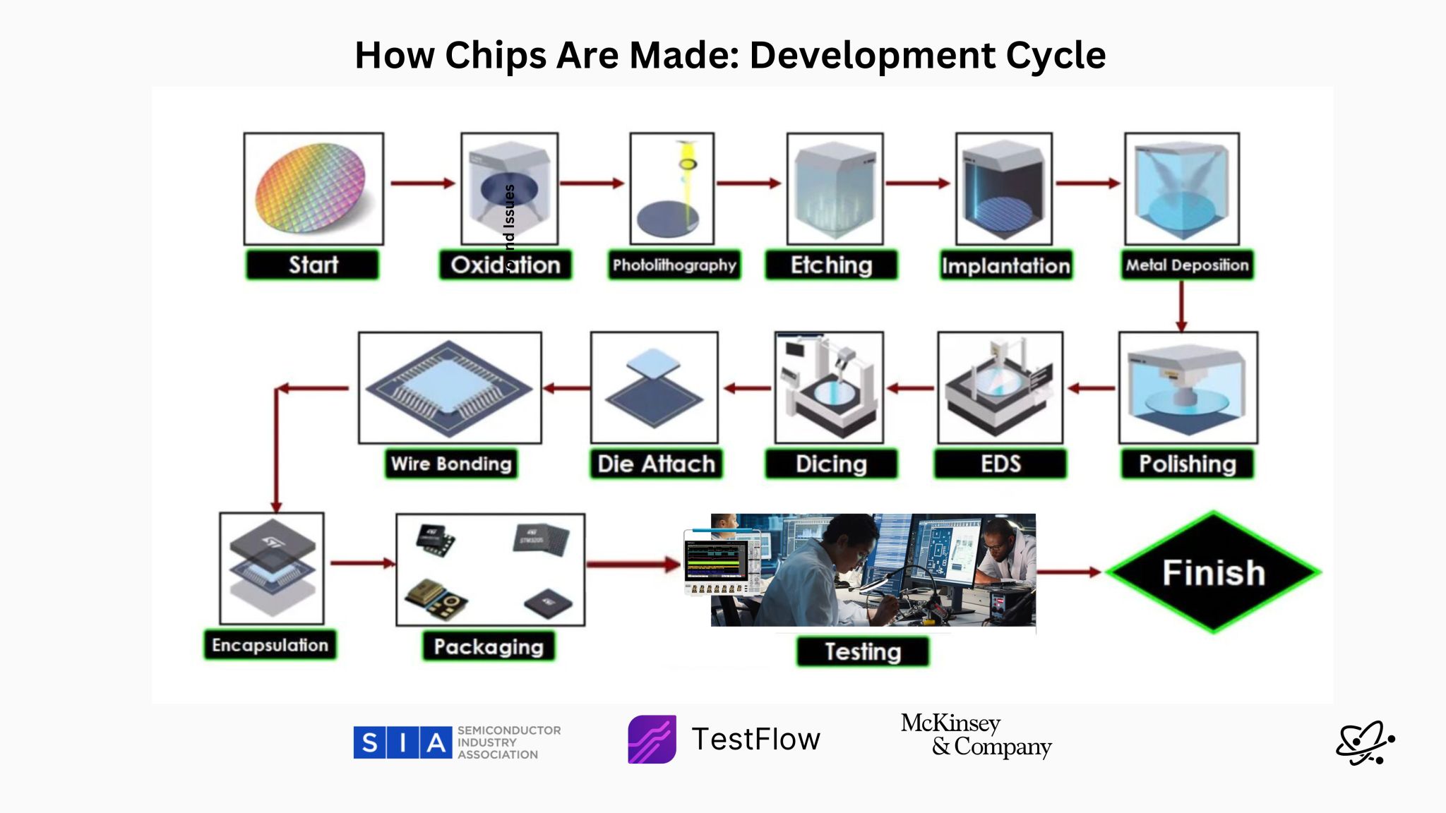
Let's walk through each major step in the semiconductor manufacturing process, from the initial silicon wafer to the final packaged chip ready for deployment.
Starting with Pure Silicon Wafer
The process begins with a pure silicon wafer, typically 300mm (12 inches) in diameter and less than 1mm thick. These wafers are grown from ultra-pure silicon crystals using the Czochralski process, achieving purity levels of 99.9999999% (nine nines).
Key Characteristics
- • 300mm diameter standard
- • Single crystal structure
- • Mirror-smooth surface
- • Precise crystallographic orientation
Quality Requirements
- • 99.9999999% purity
- • Zero surface defects
- • Uniform thickness
- • Controlled electrical properties
Oxidation Forms the Insulating Layer
The silicon wafer is heated to extremely high temperatures (800-1200°C) in the presence of oxygen or water vapor. This creates a thin layer of silicon dioxide (SiO₂) on the surface, which acts as an electrical insulator and protects the underlying silicon.
Process Details: Thermal oxidation occurs in specialized furnaces where wafers are exposed to pure oxygen or water vapor at temperatures exceeding 1000°C. The resulting oxide layer is just a few nanometers thick but provides crucial electrical isolation.
Photolithography Defines Intricate Patterns
This is perhaps the most critical step in chip manufacturing. A light-sensitive material called photoresist is applied to the wafer, then exposed to ultraviolet light through a photomask that contains the circuit patterns. The exposed areas become either more or less soluble, allowing precise pattern transfer.
Process Steps
- • Photoresist coating
- • Mask alignment
- • UV light exposure
- • Chemical development
Technology Used
- • EUV lithography (13.5nm wavelength)
- • Precision alignment systems
- • Advanced photomasks
- • Automated handling
Etching and Ion Implantation Shape Electrical Pathways
Etching removes material from areas not protected by photoresist, creating trenches and features. Ion implantation then bombards the silicon with specific atoms (dopants) to alter its electrical properties, creating the p-type and n-type regions essential for transistor operation.
Etching Process
Plasma etching uses reactive gases to remove material with atomic precision. Dry etching provides anisotropic profiles essential for modern device geometries.
Ion Implantation
High-energy ions (boron, phosphorus, arsenic) are accelerated and implanted into specific regions to create the electrical junctions needed for transistors and diodes.
Metal Deposition Builds Interconnects Layer by Layer
Multiple layers of metal interconnects are deposited to connect the transistors and other components. Modern chips can have 10+ metal layers, with copper being the primary conductor due to its low resistance and electromigration properties.
Deposition Methods
- • Physical Vapor Deposition (PVD)
- • Chemical Vapor Deposition (CVD)
- • Electroplating
- • Atomic Layer Deposition (ALD)
Materials Used
- • Copper (primary conductor)
- • Aluminum (legacy processes)
- • Tungsten (contacts and vias)
- • Barrier metals (Ta, TaN)
Chemical Mechanical Polishing (CMP)
After each layer deposition, Chemical Mechanical Polishing (CMP) ensures a perfectly flat surface. This process combines chemical etching with mechanical abrasion to achieve atomic-level smoothness, essential for subsequent layer deposition.
Critical Importance: CMP removes excess material and creates the flat surface required for photolithography. Without this step, surface variations would cause focus problems and pattern distortion in subsequent layers.
Testing and Packaging: From Wafer to Chip
After the fabrication process creates the circuit patterns on the wafer, several critical steps remain to transform the wafer into individual, functional chips ready for deployment.
Electrical Die Sort (EDS) Testing
Each individual die on the wafer undergoes comprehensive electrical testing to verify functionality. Automated probe stations make contact with test pads on each die, running thousands of tests to ensure the circuits operate within specifications.
Test Categories
- • Functional verification
- • Performance characterization
- • Power consumption testing
- • Timing verification
Test Equipment
- • Automated probe stations
- • High-speed test equipment
- • Precision measurement tools
- • Automated handling systems
Dicing Cuts Wafer into Individual Chips
The wafer is cut along predetermined scribe lines using diamond-tipped saws or laser cutting. This separates the hundreds or thousands of individual dies on the wafer, with only the dies that passed electrical testing being selected for further processing.
Precision Cutting: Dicing saws cut with tolerances measured in micrometers, ensuring clean edges and minimal damage to the delicate semiconductor structures near the die edges.
Die Attach and Wire Bonding
Individual dies are attached to lead frames or substrates using conductive adhesives. Ultra-thin gold or aluminum wires (25-50 micrometers diameter) are then bonded between the die pads and the package leads, creating electrical connections.
Die Attach Process
Dies are precisely placed and bonded using conductive epoxy or eutectic bonding, ensuring both mechanical stability and electrical connection.
Wire Bonding
Automated wire bonding machines create thousands of connections per hour, using ultrasonic or thermosonic bonding techniques for reliable electrical connections.
Encapsulation Protection
The die and wire bonds are encapsulated in protective material, typically epoxy-based molding compound. This protects the delicate semiconductor structures from mechanical damage, moisture, and thermal stress while providing the familiar chip package shape.
Protection Features
- • Moisture barrier
- • Mechanical protection
- • Thermal management
- • Chemical resistance
Package Types
- • Ball Grid Array (BGA)
- • Quad Flat Package (QFP)
- • System in Package (SiP)
- • Chip Scale Package (CSP)
Final Packaging for Shipment
The encapsulated chips receive their final package configuration, including lead trimming, forming, and plating. Package markings are laser-etched or printed, identifying the part number, date codes, and other critical information for traceability.
Quality Assurance: Each package undergoes visual inspection and electrical testing to ensure proper lead formation, marking clarity, and package integrity before final packaging.
Final Testing and Validation
Packaged chips undergo comprehensive final testing to ensure they meet all specifications. This includes functional testing, performance characterization, and reliability screening under various temperature and voltage conditions.
Test Types
- • Functional verification
- • Performance binning
- • Burn-in testing
- • Environmental stress
Quality Metrics
- • Zero defect requirements
- • Statistical process control
- • Traceability documentation
- • Reliability qualification
The Complexity Behind the Simplicity
What we've described represents a simplified view of semiconductor manufacturing. In reality, each major step consists of dozens of sub-processes, and the entire flow can involve 500+ individual process steps. Modern fabs operate 24/7 with automated systems managing thousands of wafers simultaneously through this complex sequence.
Manufacturing Challenges
Technical Challenges
- • Atomic-scale precision requirements
- • 99.99%+ process repeatability
- • Contamination control
- • Equipment maintenance and calibration
Economic Factors
- • $20+ billion fab construction costs
- • 10-12 week cycle times
- • Yield optimization pressure
- • Technology node transitions
"It's a flow that combines chemistry, physics, nanotechnology, and automation—with almost zero room for error. Every step must be executed with precision that exceeds the tolerances of most other manufacturing processes by orders of magnitude."
Beyond Manufacturing: The Post-Silicon Challenge
While the manufacturing process creates the physical chip, the journey to a working product is far from over. Even the most perfectly manufactured chip still needs to be tested, debugged, and brought to life in the lab before it can ship to market. This is where post-silicon validation becomes critical.
The complexity that makes semiconductor manufacturing so challenging doesn't disappear once the chip is packaged. In fact, it often becomes more apparent during the validation phase, where subtle interactions between design and manufacturing can manifest as unexpected behaviors that weren't predicted during simulation.
TestFlow: AI-Powered Post-Silicon Validation

At Atoms, we focus on the critical phase that comes after all this manufacturing complexity: post-silicon validation. That's what we're building with TestFlow—an AI-powered validation tool that automates the entire validation process, helping teams bring chips to market 10x faster.
While the manufacturing process creates the chip, TestFlow ensures it works reliably in real-world applications. By combining AI-powered automation with deep semiconductor expertise, we're transforming how teams validate their silicon investments and bring products to market.
The Future of Chip Manufacturing
As we push toward even smaller geometries and more complex designs, semiconductor manufacturing continues to evolve. New materials, novel device structures, and advanced packaging technologies are reshaping the industry. However, the fundamental principles—precision, cleanliness, and control—remain constant.
- Advanced Packaging: 3D stacking and chiplet architectures are changing how we think about chip integration
- New Materials: Beyond silicon, materials like gallium arsenide and indium gallium arsenide enable new capabilities
- AI-Driven Manufacturing: Machine learning is optimizing every aspect of the manufacturing process
- Quantum Devices: New physics-based devices require entirely new manufacturing approaches
Conclusion: From Sand to Silicon Marvels
The journey from a bare silicon wafer to a powerful microchip represents one of humanity's greatest technical achievements. Each step in this process requires extraordinary precision, advanced technology, and careful control to create devices that power our digital world.
Yet as we've seen, manufacturing the chip is only part of the equation. The real challenge lies in ensuring these incredibly complex devices work reliably in real-world applications. This is where post-silicon validation becomes crucial, bridging the gap between manufacturing capability and market-ready products.
As semiconductor technology continues to advance, both manufacturing precision and validation sophistication must evolve together. The companies that master both aspects—creating chips with atomic precision and validating them with AI-powered efficiency—will lead the next generation of technological innovation.
Ready to Accelerate Your Chip Validation?
Your chips have been manufactured with incredible precision. Now ensure they work flawlessly with TestFlow's AI-powered validation platform. Accelerate your time-to-market and bring your silicon investments to life faster than ever before.