In semiconductor terminology, wafer, chip, and die are often used interchangeably, but they represent distinct stages in the manufacturing process. Understanding these differences is crucial for anyone working in chip testing, validation, or semiconductor manufacturing.
Whether you're new to semiconductors or need to clarify these fundamental concepts, this guide breaks down the silicon hierarchy from raw wafer to finished chip. Let's explore each stage and understand why these distinctions matter for chip validation and testing.
The Pizza Analogy: A Simple Way to Remember
Visual Analogy
The wafer is a pizza — a large, circular base that's perfectly prepared and ready for processing.
Each die is a slice — individual portions cut from the pizza, each containing the same ingredients and functionality.
The chip is that slice boxed and ready to deliver — packaged, protected, and prepared for the end customer.
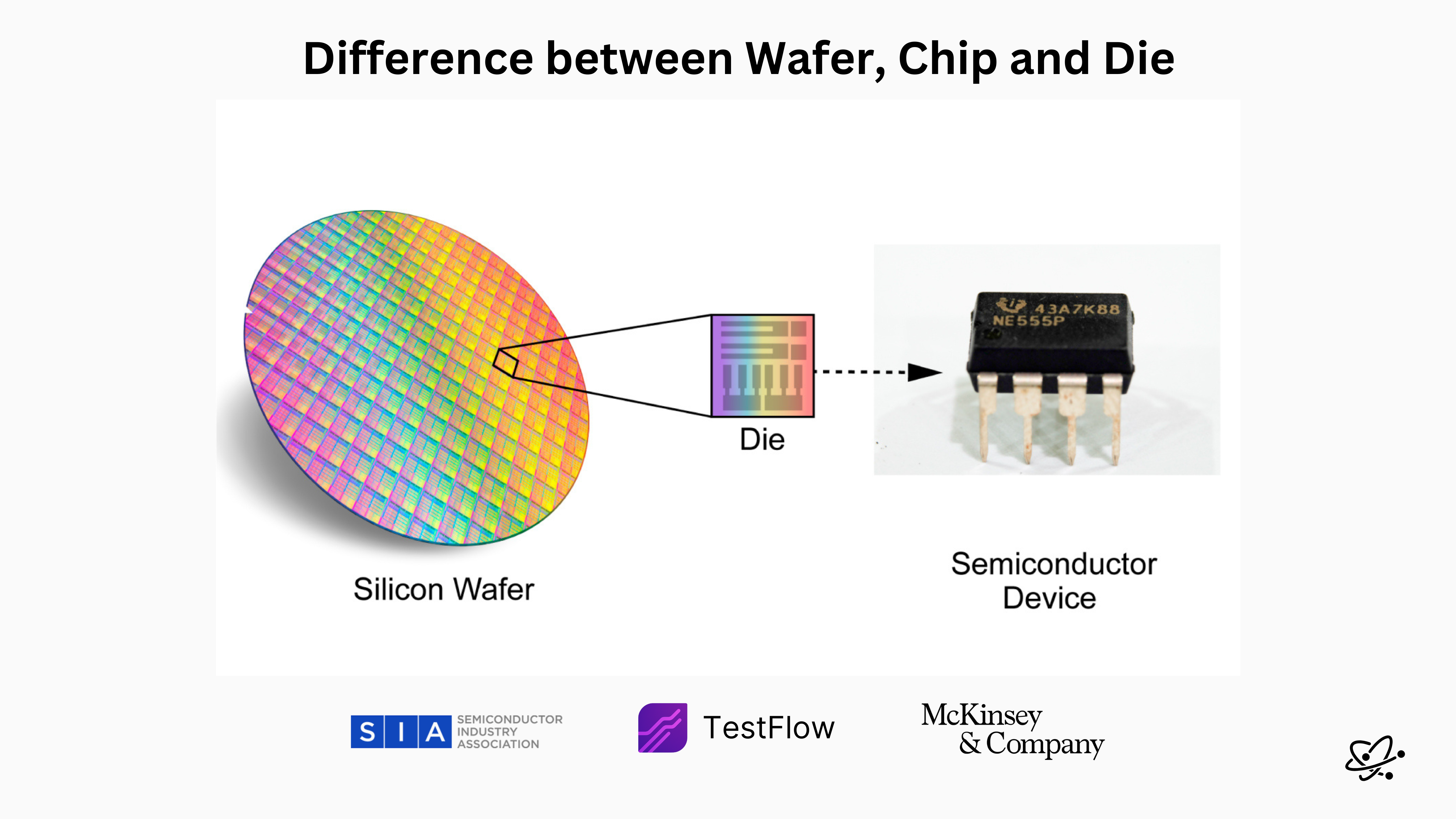
1. Wafer: The Raw Canvas
A wafer is a thin, circular slice of pure silicon that serves as the foundation for fabricating integrated circuits. Think of it as the canvas where thousands of tiny circuits are etched layer by layer using advanced photolithography.
Wafer Specifications
Physical Properties:
- • Diameter: 200mm or 300mm (most common)
- • Thickness: 0.5-1.0mm typically
- • Material: Ultra-pure silicon (99.9999999%)
- • Surface: Mirror-polished finish
Manufacturing Details:
- • Crystal orientation: Usually (100) or (111)
- • Resistivity: Varies by application
- • Flatness: Critical for lithography
- • Contamination: Parts per billion levels
Example: A polished 300mm silicon wafer before any chip fabrication begins. At this stage, it's just pure silicon with no circuits—ready to become the foundation for hundreds or thousands of individual chips.
"A single 300mm wafer can contain over 1,000 individual processor dies, each capable of becoming a complete CPU after packaging."
2. Die: The Core Logic Unit
A die is a single block of circuitry on the wafer—essentially one instance of the chip design. After the wafer is processed through hundreds of manufacturing steps, it's cut into individual dies, each capable of performing the full functionality intended.
Die Characteristics
Each die contains the complete circuit design—whether it's a processor core, memory controller, graphics unit, or specialized accelerator. The die size directly impacts cost, yield, and performance.
- • Contains complete functional circuits
- • Size ranges from 10mm² to 800mm²+
- • Billions of transistors per die
- • Tested before packaging
Die Testing
Dies undergo extensive testing while still on the wafer (wafer-level testing) to identify functional units before the expensive packaging process. This is where TestFlow excels in automated validation.
- • Functional verification testing
- • Performance characterization
- • Defect screening
- • Yield optimization
Example: One processor core on a multi-core CPU wafer. Each die contains identical circuitry but may perform differently due to manufacturing variations—this is why chips are often binned into different performance tiers.
3. Chip (or Package): The Finished Product
A chip is the packaged version of the die, complete with protective housing, heat management, and electrical connections. It's what gets shipped to customers and installed in devices—from smartphones to data center servers.
Packaging Process
The packaging process transforms a delicate die into a robust, connectable component:
Die Attachment
The die is mounted onto a substrate or lead frame using specialized adhesives or solders.
Wire Bonding
Ultra-thin wires (25-50 microns) connect the die's bond pads to the package pins, enabling electrical connectivity.
Encapsulation
The die and wires are encapsulated in protective material (plastic, ceramic, or metal) to prevent damage and contamination.
Final Testing
Comprehensive testing ensures the packaged chip meets all specifications before shipping to customers.
Example: An Intel Core i9 CPU installed on a motherboard. The die inside contains the processor cores, but the package provides the pins, heat spreader, and protection needed for real-world use.
Why These Distinctions Matter for Chip Testing
Understanding the wafer-to-chip hierarchy is crucial for effective chip testing and validation strategies:
| Stage | Testing Focus | Key Challenges | TestFlow Solutions |
|---|---|---|---|
| Wafer | Process monitoring, uniformity | Across-wafer variations | Statistical process control |
| Die | Functional verification, sorting | High-volume testing, probe contact | Automated test generation |
| Chip | Final validation, characterization | Package effects, thermal management | Comprehensive test suites |

TestFlow: Testing Across the Silicon Hierarchy
From wafer-level screening to final chip validation, TestFlow provides comprehensive testing solutions for every stage
Common Misconceptions and Clarifications
❌ Misconception: "Chip and die are the same thing"
✅ Reality: A die is the bare silicon circuit, while a chip includes the packaging, connections, and protection. The die is what's inside the chip package.
❌ Misconception: "All dies on a wafer are identical"
✅ Reality: While the circuit design is identical, manufacturing variations mean each die performs slightly differently. This is why testing and binning are crucial.
❌ Misconception: "Wafer testing isn't necessary if you test the final chip"
✅ Reality: Wafer-level testing is essential for identifying good dies before expensive packaging. It's much more cost-effective to discard a defective die than a packaged chip.
The Economics of the Silicon Hierarchy
Understanding the cost implications at each stage helps explain why testing strategies are so important:
Wafer Costs
A 300mm wafer for advanced nodes:
- • Raw wafer: $1,000-$2,000
- • Processing: $10,000-$20,000
- • Total per wafer: $15,000-$25,000
Die Economics
Per die cost depends on:
- • Die size (larger = more expensive)
- • Yield (defects increase cost)
- • Typical range: $50-$500 per die
Packaging Costs
Package adds significant value:
- • Simple packages: $5-$20
- • Advanced packages: $50-$200+
- • Testing: $2-$10 per unit
"Catching a defective die at wafer level saves $50-$200 in packaging costs. This is why comprehensive wafer-level testing is so critical for semiconductor profitability."
TestFlow's Role in the Silicon Hierarchy
TestFlow provides comprehensive testing solutions that span the entire silicon hierarchy, from wafer to final chip validation:
Comprehensive Testing Coverage
Wafer-Level Testing:
- • Process control monitoring
- • Parametric testing automation
- • Statistical analysis and reporting
- • Yield optimization insights
Die and Chip Testing:
- • Automated test generation
- • Functional verification suites
- • Performance characterization
- • Comprehensive reporting
Conclusion: Mastering the Silicon Hierarchy
Understanding the distinction between wafer, die, and chip is fundamental to working effectively in the semiconductor industry. Each stage has unique characteristics, challenges, and testing requirements:
- Wafers are the foundation—pure silicon canvases where circuits are built
- Dies are individual functional units—the core logic that makes chips work
- Chips are the final products—packaged, protected, and ready for integration
For chip testing and validation, understanding this hierarchy enables more effective testing strategies, better cost management, and improved yield optimization. Whether you're screening dies at wafer level or validating final chip performance, each stage requires specialized approaches and tools.
Optimize Your Silicon Testing Strategy
TestFlow provides comprehensive testing solutions across the entire silicon hierarchy—from wafer-level screening to final chip validation. Reduce costs, improve yields, and accelerate time-to-market with intelligent test automation.