As Moore's Law reaches its physical limits, the semiconductor industry is pivoting to system-level innovation through advanced packaging techniques. Meanwhile, choosing between microprocessors and microcontrollers remains a fundamental design decision. This comprehensive guide explores both critical aspects of modern semiconductor design and their validation challenges.
Part I: Advanced Packaging - Beyond Moore's Law
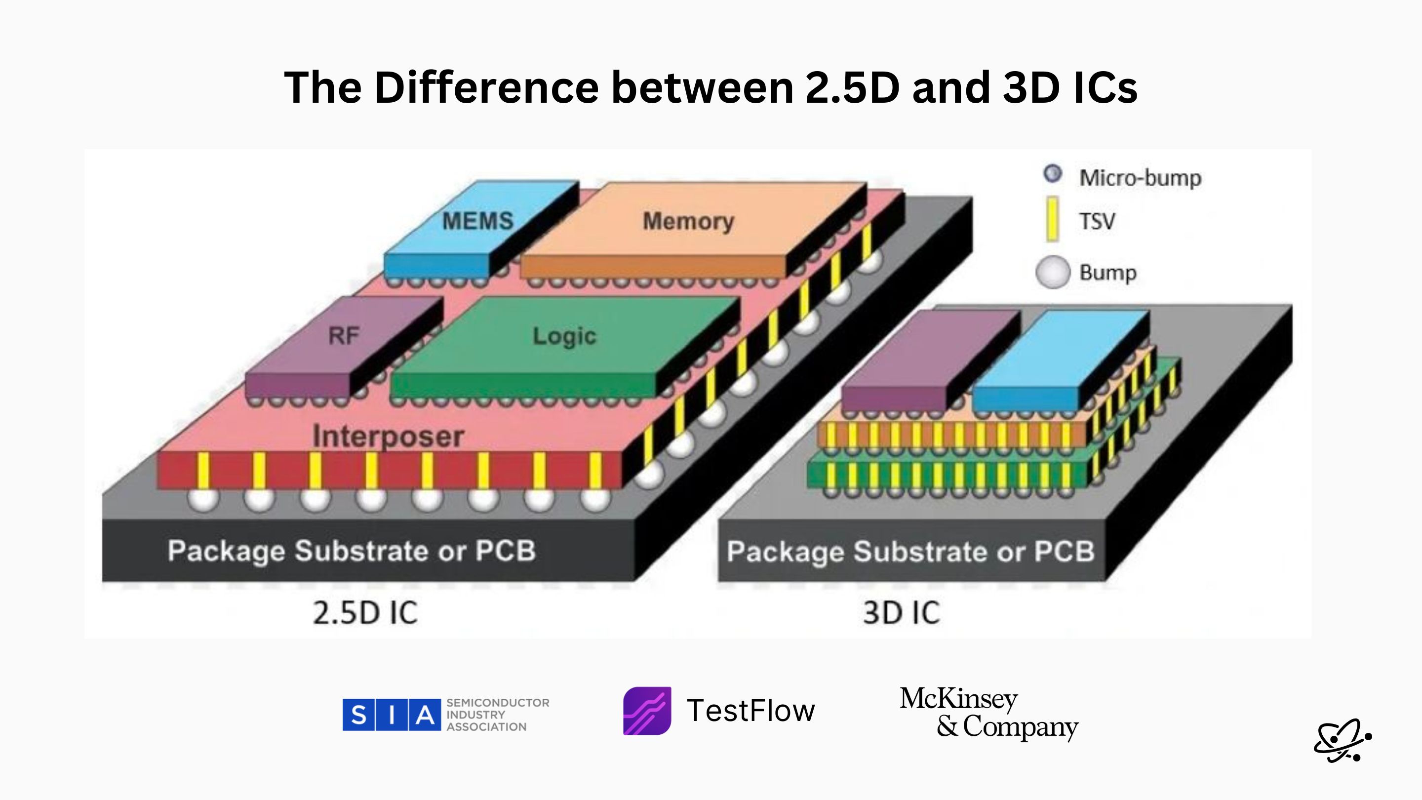
As traditional node scaling becomes increasingly expensive and technically challenging, the semiconductor industry has shifted focus to advanced packaging as the new performance lever. Two approaches dominate this landscape: 2.5D and 3D integrated circuits.
2.5D Integration
In 2.5D packaging, chips are placed side-by-side on a common interposer—typically made of silicon or glass—which routes high-speed connections between them. Think of it as horizontal integration with significantly higher bandwidth and lower latency than traditional PCB connections.
Higher bandwidth density without the thermal challenges of vertical stacking
3D Integration
3D ICs stack chips vertically and connect them using TSVs (Through-Silicon Vias)—tiny vertical tunnels through silicon that create the shortest possible communication paths between layers. This approach maximizes density and performance in minimal footprint.
Maximum density and shortest interconnect paths for ultimate performance
The City vs Skyscraper Analogy
2.5D is like a sprawling city
Buildings (chips) spread across one giant floor, connected by high-speed roads (interposer traces). Easy to cool, expandable, but takes more space.
3D is like a skyscraper
Floors (chips) stacked with elevators (TSVs) moving data vertically. Faster, denser, but harder to cool and more complex to build.
Technical Deep Dive: How Advanced Packaging Works
Understanding the technical implementation of these approaches is crucial for design engineers and validation teams working with next-generation semiconductor systems.
Interposer Technology
Silicon interposers in 2.5D packages provide ultra-fine pitch interconnects (as small as 2μm) enabling massive parallel connections between dies. Glass interposers offer lower cost for less demanding applications.
Through-Silicon Vias
TSVs in 3D packages are vertical conductors with diameters ranging from 1-20μm, enabling direct chip-to-chip connections. They reduce interconnect length by up to 1000x compared to wire bonds.
Thermal Management
Advanced packaging requires sophisticated thermal solutions. 2.5D allows easier heat spreading, while 3D needs micro-cooling channels and thermal TSVs to manage hotspots.
Where Advanced Packaging is Used Today
Advanced packaging has moved from research labs to production, powering some of today's most demanding applications:
| Technology | Applications | Key Players | Benefits |
|---|---|---|---|
| 2.5D ICs | AMD GPUs, Xilinx FPGAs, HBM-connected AI accelerators | AMD, Intel, NVIDIA, Xilinx | High bandwidth, better yields |
| 3D ICs | Intel Foveros, Samsung HBM, Apple M-series, Edge AI | Intel, Samsung, Apple, SK Hynix | Maximum density, lowest latency |
"It's not just about smaller nodes anymore. Packaging is becoming the new performance lever—and how you connect dies matters as much as what you put on them."
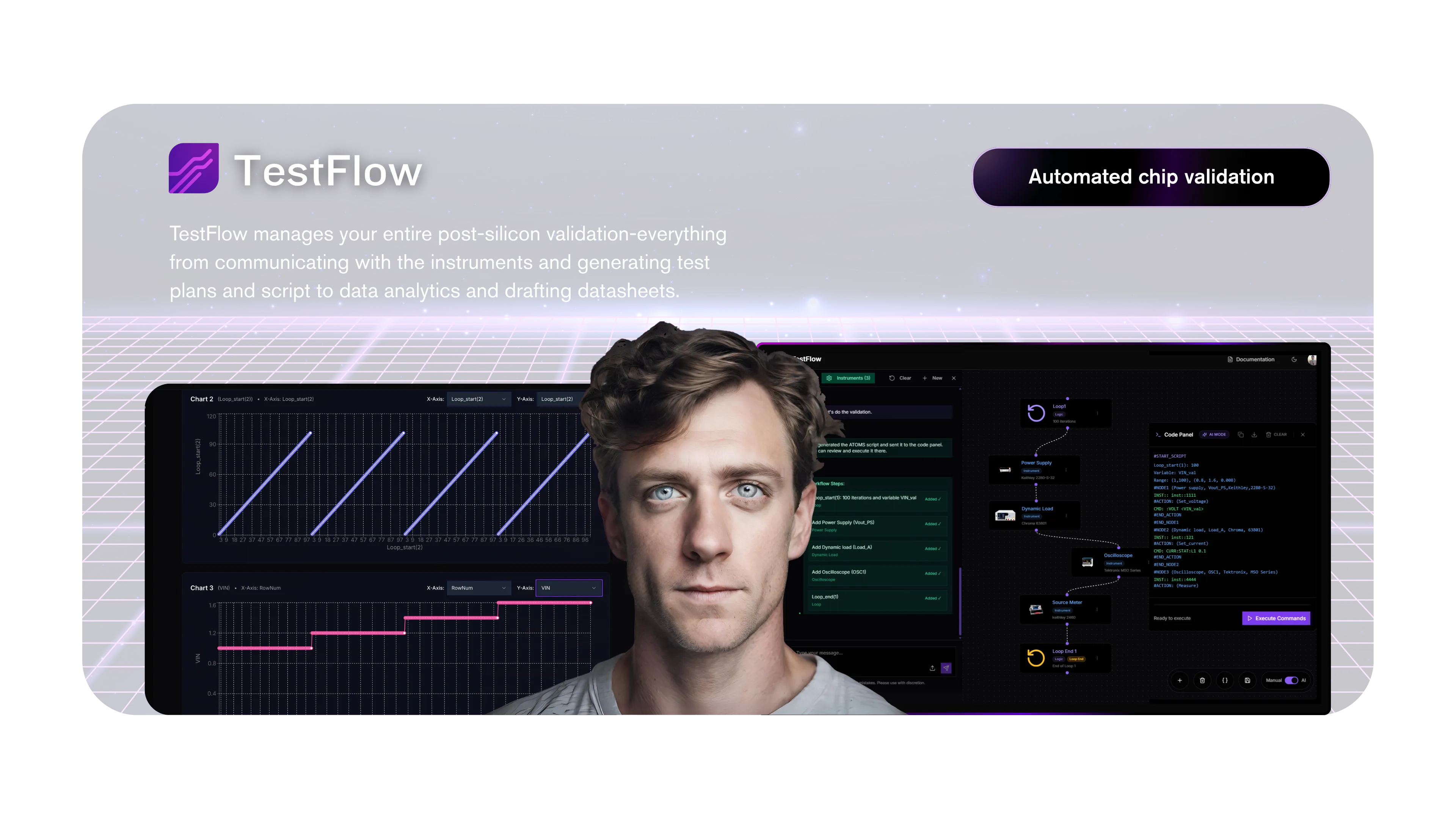
TestFlow: Validating Advanced Packaging
AI-powered validation platform specifically designed to handle the complexity of 2.5D and 3D IC validation challenges
Validation Challenges in Advanced Packaging
Advanced packaging introduces unique validation challenges that traditional testing approaches struggle to address effectively. TestFlow's AI-powered platform is specifically designed to tackle these complex validation scenarios.
Traditional Validation Challenges
- • Complex thermal interactions between stacked dies
- • Signal integrity across multiple interconnect layers
- • Power delivery network validation in 3D structures
- • Mechanical stress testing of TSV structures
- • Cross-talk and electromagnetic interference
TestFlow Solutions
- • AI-driven thermal simulation and hotspot prediction
- • Multi-layer signal integrity analysis
- • Automated power delivery validation
- • Stress-aware TSV reliability testing
- • Advanced EMI/EMC validation workflows
TestFlow Advanced Packaging Validation Process
Multi-Physics Analysis
TestFlow simultaneously analyzes thermal, electrical, and mechanical interactions across all packaging layers, identifying potential failure modes that single-domain analysis might miss.
AI-Powered Test Generation
The platform automatically generates test vectors optimized for advanced packaging structures, focusing on critical paths and potential failure modes unique to 2.5D and 3D architectures.
Predictive Reliability Assessment
Machine learning models predict long-term reliability based on stress patterns, thermal cycling, and interconnect degradation specific to advanced packaging technologies.
Part II: Microprocessors vs Microcontrollers - Choosing the Right Brain
While advanced packaging represents the cutting edge of semiconductor technology, the fundamental choice between microprocessors and microcontrollers remains crucial for system design. Understanding their differences is key to making informed architecture decisions.
Microprocessor
General-Purpose Compute EngineMicroprocessors are designed for maximum computational flexibility and performance. They excel at running complex operating systems, applications, and handling diverse workloads.
Microcontroller
Specialized Task ControllerMicrocontrollers integrate CPU, memory, and peripherals on a single chip, optimized for specific control tasks and embedded applications.
The House Building Analogy
Microprocessor = The Architect's Blueprint
Designed to handle everything, but needs contractors and workers (external components) to actually build the system. Powerful and flexible, but requires a full support ecosystem.
Microcontroller = Smart Thermostat
Self-contained, optimized for a specific task, and ready to plug in. Everything needed is built-in, making it perfect for dedicated control applications.
Detailed Comparison: When to Choose What
| Aspect | Microprocessor | Microcontroller |
|---|---|---|
| Primary Use | PCs, smartphones, servers | Embedded systems, IoT, appliances |
| Architecture | CPU only, external components needed | CPU + RAM + Storage + I/O integrated |
| Performance | High computational power (GHz) | Moderate performance (MHz), real-time focused |
| Power Consumption | High (watts to hundreds of watts) | Low (milliwatts to watts) |
| Cost | High (system cost including peripherals) | Low (single-chip solution) |
| Development | Complex OS development | Firmware/bare-metal programming |
Real-World Applications
Understanding where each technology excels helps inform design decisions:
Microprocessor Applications
- • Desktop and laptop computers
- • Smartphones and tablets
- • Data center servers
- • High-performance workstations
- • Gaming consoles
- • AI/ML training systems
Microcontroller Applications
- • Automotive engine control units
- • Home appliances (washing machines, microwaves)
- • IoT sensors and devices
- • Industrial automation systems
- • Medical devices and wearables
- • Smart home controllers
"Microprocessors run your laptop. Microcontrollers run your coffee machine. And both are essential to the modern tech stack."
Validation Considerations for Both Technologies
Whether validating advanced packaging solutions or choosing between microprocessors and microcontrollers, comprehensive testing is crucial. TestFlow provides validation solutions optimized for both scenarios.
Advanced Packaging Validation
Complex multi-die systems require sophisticated validation approaches that can handle thermal, electrical, and mechanical interactions across multiple layers and interconnect technologies.
Microprocessor/Microcontroller Testing
Each architecture requires tailored validation approaches—high-performance testing for microprocessors and real-time, low-power validation for microcontrollers.
The Future Convergence
Interestingly, advanced packaging and the microprocessor/microcontroller distinction are beginning to converge. Modern systems increasingly use heterogeneous integration—combining different types of processors in advanced packaging configurations.
Heterogeneous Integration Examples
- Apple M-series: CPU, GPU, and specialized processors in advanced packaging
- Intel Lakefield: High-performance and efficiency cores in 3D packaging
- Edge AI systems: Microcontrollers with AI accelerators in 2.5D packages
- Automotive SoCs: Safety microcontrollers with high-performance processors
Conclusion: The New Era of Semiconductor Design
The semiconductor industry is entering a new era where advanced packaging techniques like 2.5D and 3D integration are enabling system-level innovations that pure node scaling cannot achieve. Simultaneously, the fundamental choice between microprocessors and microcontrollers continues to shape how we approach different application domains.
Success in this new landscape requires not just understanding these technologies individually, but recognizing how they can be combined to create optimized solutions. Advanced packaging enables the integration of different processor types, memory technologies, and specialized accelerators in ways that maximize performance while minimizing power and footprint.
As these technologies become more complex, validation becomes increasingly critical. TestFlow's AI-powered platform is designed to handle the unique challenges of both advanced packaging validation and comprehensive processor testing, ensuring that these sophisticated systems work flawlessly in real-world applications.
Ready to Validate Your Next-Generation Design?
Whether you're working with advanced packaging technologies or choosing the right processor architecture, TestFlow provides the AI-powered validation tools you need to ensure success. Our platform is specifically designed to handle the complexity of modern semiconductor systems.