8 Layers of the Semiconductor Industry: Inside the $1 Trillion Chip Ecosystem
From raw materials to final systems, the semiconductor industry is a global relay race where each layer is critical and each player irreplaceable. Discover the 8 essential layers that power our digital world.
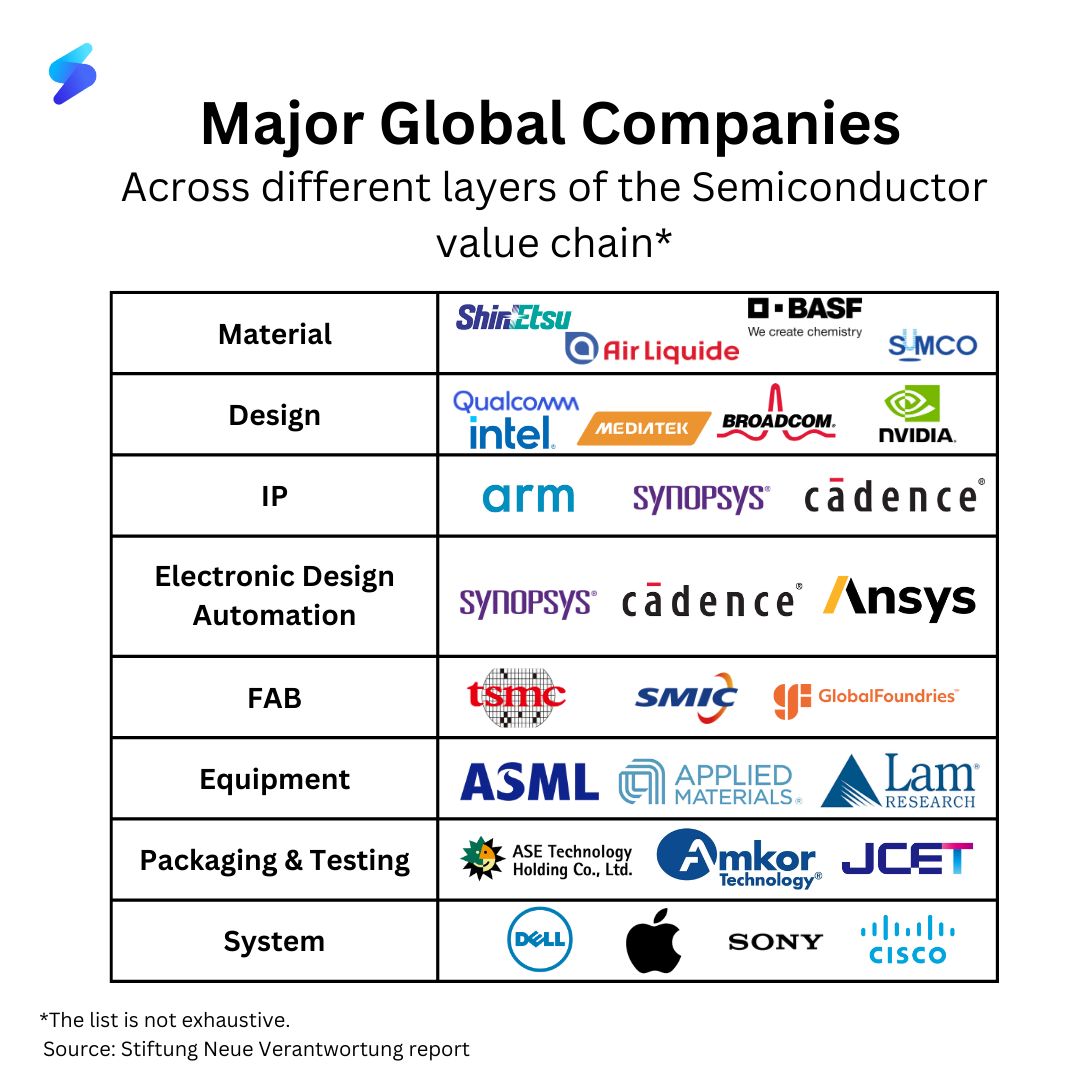
The semiconductor industry isn't dominated by a single company—it's a deep, interconnected stack of specialized players, each mastering a critical piece of the chip creation puzzle. From the pure silicon wafers that form the foundation to the complex systems that end up in your smartphone, this $1 trillion ecosystem represents one of humanity's most sophisticated supply chains.
Understanding these 8 layers is crucial for anyone working in technology, as disruption in any single layer can ripple across the entire global tech ecosystem. Let's explore how this intricate machine works.
The Semiconductor Industry Stack
System Companies
Final products you use daily
Apple
iPhones, Macs, iPads
Dell
PCs, Servers
Sony
PlayStation, TVs
Cisco
Networking equipment
These companies integrate chips into complete systems that consumers and businesses use. They drive demand for semiconductors and define performance requirements.
Packaging & Testing (OSAT)
Connecting dies to the real world
ASE Group
World's largest OSAT
Amkor
Advanced packaging
JCET
Chinese OSAT leader
SPIL
Memory packaging
OSATs handle the final assembly, packaging, and testing of semiconductor chips before they ship to customers. They ensure chips work correctly and can survive real-world conditions.
Equipment Vendors
Machines that print at nanometer scale
ASML
EUV lithography
Applied Materials
Deposition, etch
Lam Research
Plasma etching
KLA
Process control
These companies build the ultra-complex machines that fabricate chips. ASML's EUV scanners cost $200M each and are essential for advanced nodes.
Foundries & IDMs
The most complex factories in the world
TSMC
62% foundry share
Samsung
Memory + foundry
GlobalFoundries
Mature nodes
Intel
IDM + foundry
Foundries manufacture chips designed by other companies, while IDMs design and manufacture their own. These fabs cost $20B+ and take 3-5 years to build.
EDA Tools
The invisible engines of chip creation
Synopsys
Design, verification
Cadence
Analog, digital
Siemens EDA
Verification, test
TestFlow
AI validation
EDA tools enable engineers to design, simulate, and verify billion-transistor chips. Without these software platforms, modern chip design would be impossible.
IP Cores
Reusable logic blocks and processor cores
Arm
CPU architectures
Imagination
GPU cores
Rambus
Memory interfaces
CEVA
DSP cores
IP companies create reusable building blocks that chip designers license and integrate into their SoCs. Arm's CPU cores power 95% of smartphones.
Fabless Design Companies
The brains behind the architecture
Qualcomm
Mobile SoCs
NVIDIA
GPUs, AI chips
AMD
CPUs, GPUs
Broadcom
Networking, RF
Fabless companies focus purely on chip design and outsource manufacturing to foundries. This model enables innovation without massive capital investment.
Raw Materials
Where it all begins—chemicals, wafers, gases
Shin-Etsu
Silicon wafers
BASF
Chemicals
Air Liquide
Process gases
Sumco
Silicon substrates
Materials companies provide the ultra-pure silicon wafers, chemicals, and gases that make chip manufacturing possible. Quality here determines yield downstream.
Critical Interdependencies
How the Layers Connect
Material Quality → Chip Yield
Ultra-pure silicon wafers and chemicals directly impact manufacturing yield rates
EDA Tools → Design Complexity
Advanced software enables billion-transistor designs that would be impossible manually
Equipment Innovation → Process Nodes
ASML's EUV technology enables 7nm, 5nm, and 3nm manufacturing
System Demand → Innovation Cycles
Consumer electronics drive requirements that cascade through all layers
Single Points of Failure
Critical Bottlenecks
- • ASML: Only supplier of EUV lithography
- • TSMC: 62% of foundry capacity
- • Taiwan: 63% of global chip production
- • Shin-Etsu: Major silicon wafer supplier
Risk Mitigation
- • Geographic diversification efforts
- • Strategic inventory management
- • Alternative supplier development
- • Government policy support
Economic Impact by Layer
Market Size by Layer (2024)
Growth Trends
AI/ML driving system demand
Equipment CAGR (2024-2030)
Overall semiconductor CAGR
Future Evolution of the Stack
Emerging Trends
New Layer: AI Validation
AI-powered validation and testing platforms are becoming a distinct layer, automating complex chip validation processes.
Chiplet Ecosystem
Modular chip architectures are creating new players focused on chiplet design and integration.
Consolidation vs. Specialization
Consolidation Trends
- • Foundry market concentrating in TSMC
- • EDA dominated by 3 major players
- • Equipment consolidation around leaders
- • Vertical integration by system companies
New Specializations
- • AI-specific chip architectures
- • Edge computing optimizations
- • Quantum-classical hybrid systems
- • Sustainability-focused processes
The Intricate Machine of Innovation
The semiconductor industry's 8-layer structure represents one of humanity's most complex and sophisticated supply chains. Each layer depends on the others, creating a delicate ecosystem where innovation in one area can transform entire industries.
Understanding these interdependencies is crucial for anyone working in technology. A disruption in materials can affect chip yields; advances in EDA tools enable new architectures; equipment breakthroughs unlock smaller process nodes; and system demand drives innovation throughout the stack.
As we move toward an AI-driven future, this 8-layer structure continues to evolve, with new specializations emerging and traditional boundaries blurring. The companies that master multiple layers—or create entirely new ones—will shape the next chapter of technological progress.
Optimize Your Layer in the Stack
Whether you're designing chips, manufacturing them, or validating their performance, TestFlow's AI-powered platform helps optimize your role in the semiconductor ecosystem. Join the companies revolutionizing chip validation.