How Much Does a 2nm Chip Really Cost? $725M Development Breakdown
We often talk about Moore's Law, but rarely about its cost. Discover why developing a 2nm chip now costs $725 million—and why validation has become the fastest-growing expense in advanced semiconductor design.
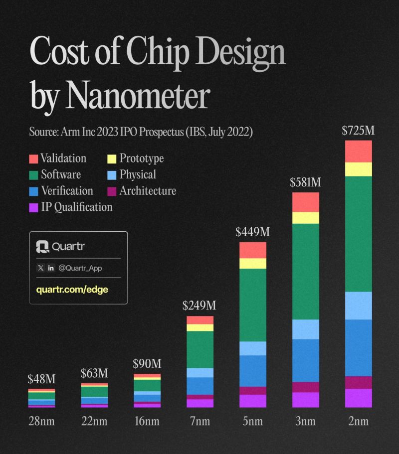
Moore's Law isn't just about transistor density—it's about economics. While we celebrate each new process node for its performance gains, the financial reality behind these advances tells a sobering story. Developing a chip on the latest 2nm process node now costs an staggering $725 million, representing a 25% increase from 3nm and a 15x jump from 28nm designs.
But where does all this money go? And why is validation emerging as the fastest-growing cost component in advanced chip design? Let's break down the economics of bleeding-edge semiconductor development.
The Exponential Cost Curve
Development Cost by Process Node
Cost Growth Analysis
Cost increase from 28nm to 2nm
Average cost increase per node
Validation costs at 2nm
Where the $725M Goes: Complete Cost Breakdown
Architecture & Design (25% - $181M)
System Architecture
- • CPU/GPU core design: $45M
- • Memory hierarchy optimization: $25M
- • Interconnect architecture: $20M
- • Power management design: $15M
Design Engineering
- • RTL design and coding: $35M
- • Design team salaries (3 years): $25M
- • Architecture research: $11M
IP Qualification & Verification (20% - $145M)
IP Licensing & Development
- • ARM CPU cores: $40M
- • GPU IP licensing: $25M
- • Interface IP (PCIe, DDR): $15M
- • Custom IP development: $20M
Verification & Testing
- • Functional verification: $25M
- • Formal verification: $15M
- • System-level testing: $5M
Physical Design & Implementation (18% - $130M)
Physical Implementation
- • Floor planning and placement: $30M
- • Routing and optimization: $25M
- • Clock tree synthesis: $15M
- • Power grid design: $20M
Design Closure
- • Timing closure: $20M
- • Power optimization: $15M
- • Physical verification: $5M
Validation & Testing (22% - $159M)
Post-Silicon Validation
- • Silicon bring-up and debug: $45M
- • Performance characterization: $30M
- • Power and thermal testing: $25M
- • Reliability testing: $20M
System Integration
- • Software validation: $25M
- • System-level testing: $14M
Note: Validation costs have grown 300% since 7nm due to increased complexity
Tools & Infrastructure (15% - $110M)
EDA Tool Licenses
- • Synopsys tool suite: $35M
- • Cadence tool suite: $30M
- • Mentor/Siemens EDA: $15M
- • Specialized tools: $10M
Compute Infrastructure
- • High-performance servers: $15M
- • Cloud computing costs: $5M
The Validation Crisis: Why Testing Costs Are Exploding
Validation Cost Evolution
Why Validation Costs Are Exploding
Exponential Complexity
2nm chips have 50B+ transistors requiring comprehensive testing
New Failure Modes
Advanced nodes introduce novel reliability challenges
Tighter Margins
Smaller process variations require more precise testing
System Integration
Complex SoCs need extensive system-level validation
Validation Bottlenecks
Manual Testing
70% of validation still requires manual intervention
Debug Time
Root cause analysis can take weeks per critical bug
Test Coverage
Achieving 99%+ coverage requires exponential effort
Time Pressure
Validation delays can cost $1M+ per week
AI-Powered Validation: The Solution
Advanced validation platforms like TestFlow are addressing the validation crisis by automating complex test scenarios, reducing debug time by 70%, and enabling comprehensive coverage of 2nm designs. AI-driven testing is becoming essential for managing the complexity of bleeding-edge chips.
Learn About Advanced ValidationEconomic Implications: Who Can Afford 2nm?
Break-Even Analysis
Minimum Volume
Units needed to amortize $725M development cost
Break-Even Time
Typical payback period for 2nm investments
Market Requirement
Annual revenue needed to justify 2nm development
Who Can Afford 2nm Development?
Viable Candidates
Challenging Economics
Industry Impact: The Great Consolidation
Market Concentration Effects
Barriers to Entry
- • $725M development cost eliminates smaller players
- • Only companies with massive volumes can justify investment
- • Technology gap widens between leaders and followers
- • Innovation becomes concentrated in few companies
Strategic Responses
- • Chiplet architectures to share development costs
- • Longer product lifecycles to amortize investment
- • Focus on specialized markets with premium pricing
- • Strategic partnerships and joint development
The Future of Semiconductor Economics
Companies that can afford 2nm development
Estimated cost for 1nm development
Market share controlled by top 3 players
The $725M Reality Check
The $725 million cost of 2nm chip development represents more than just inflation—it's a fundamental shift in semiconductor economics. We're witnessing the end of Moore's Law as an economically viable scaling strategy for most companies, replaced by a new reality where only the largest technology giants can afford to push the boundaries of silicon.
The explosion in validation costs, now representing 22% of total development expenses, reflects the growing complexity of modern chips. As transistors shrink and designs become more sophisticated, ensuring they work correctly becomes exponentially more challenging and expensive.
This economic reality is reshaping the entire semiconductor industry, concentrating innovation in the hands of a few companies while forcing others to find alternative strategies. The companies that master both advanced design and efficient validation will define the next era of computing.
Reduce Your Validation Costs
Don't let validation become your biggest bottleneck. TestFlow's AI-powered platform can reduce validation time and costs by up to 70%, making advanced node development more economically viable.