2.5D vs 3D ICs: The Difference Between Horizontal and Vertical Integration
As Moore's Law slows, the industry is shifting to system-level innovation through advanced packaging. Discover the critical differences between 2.5D and 3D IC architectures and why they're revolutionizing semiconductor design.
As traditional silicon scaling approaches its physical limits, the semiconductor industry is pioneering new approaches to continue performance improvements. Advanced packaging technologies, particularly 2.5D and 3D integrated circuits, represent the next frontier in semiconductor innovation—moving beyond Moore's Law through clever integration rather than just smaller transistors.
These technologies aren't just academic concepts—they're powering today's most advanced processors, from AMD's chiplet-based CPUs to Apple's M-series processors. Understanding the differences between 2.5D and 3D integration is crucial for anyone involved in modern semiconductor design.
2.5D ICs: Horizontal Integration Revolution
The City Analogy
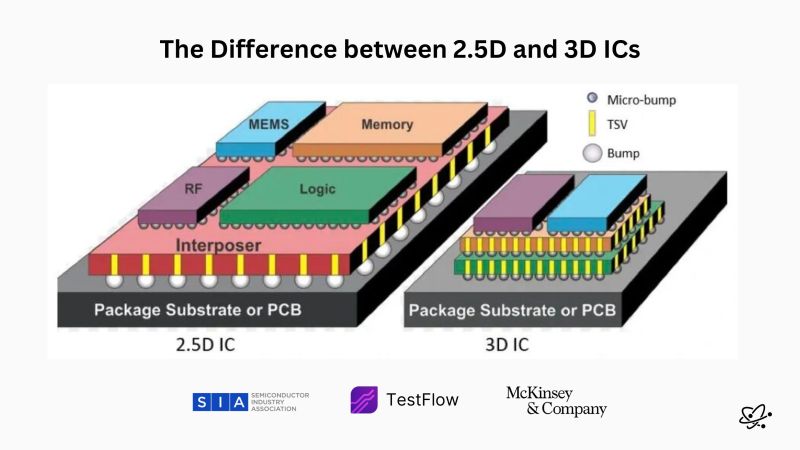
Think of 2.5D ICs as a city spread across one giant floor—multiple buildings (chips) connected by high-speed roads (interposer traces). Chips are placed side-by-side on a common interposer (silicon or glass), which routes connections between them with much higher bandwidth and lower latency than traditional PCBs.
Key Characteristics
- • Chips mounted side-by-side on interposer
- • Silicon or glass interposer substrate
- • High-density interconnect routing
- • Shorter interconnect lengths than PCB
- • Heterogeneous chip integration
- • Known good die (KGD) requirement
Technical Advantages
- • 10-100x higher interconnect density
- • Reduced parasitic capacitance
- • Lower power consumption
- • Better signal integrity
- • Improved thermal management
- • Mix different process technologies
2.5D Implementation Examples
AMD Ryzen/EPYC
Chiplet architecture with I/O die and compute chiplets
Xilinx FPGAs
FPGA fabric with HBM memory stacks
NVIDIA AI GPUs
GPU dies with HBM memory integration
3D ICs: Vertical Integration Breakthrough
The Skyscraper Analogy
3D ICs are like skyscrapers—floors (chips) stacked vertically with elevators (Through-Silicon Vias or TSVs) moving data between layers. This approach offers the ultimate in density and performance but presents significant thermal and manufacturing challenges.
Core Technologies
- • TSVs: Vertical connections through silicon
- • Wafer Bonding: Direct wafer-to-wafer attachment
- • Thinning: Ultra-thin wafer processing
- • Alignment: Precise layer-to-layer registration
- • Testing: Layer-by-layer validation
Performance Benefits
- • Shortest possible interconnect lengths
- • Maximum integration density
- • Reduced power consumption
- • Fastest inter-chip communication
- • Smallest form factor
3D IC Implementation Examples
Intel Foveros
3D chiplet integration with active interposer
Samsung HBM
Stacked memory with TSV connections
Apple M-Series
Unified memory architecture with 3D elements
2.5D vs 3D: Head-to-Head Comparison
Comprehensive Comparison Matrix
| Aspect | 2.5D ICs | 3D ICs |
|---|---|---|
| Integration Density | High | Very High |
| Interconnect Length | Short | Shortest |
| Thermal Management | Good | Challenging |
| Manufacturing Complexity | Medium | High |
| Cost | Medium | High |
| Testing Complexity | Medium | Very High |
| Yield Impact | Low | Medium |
| Market Maturity | Production Ready | Emerging |
Technical Implementation Details
2.5D Interposer Technology
Silicon Interposer
- • High-density routing layers (10-12 metal layers)
- • Fine-pitch interconnects (2-5 μm)
- • Through-silicon vias for power/ground
- • Excellent electrical performance
- • Compatible with standard processes
Glass Interposer
- • Lower cost than silicon
- • Better thermal properties
- • Larger panel sizes possible
- • Lower electrical losses
- • Emerging technology option
3D IC Through-Silicon Via (TSV) Technology
TSV Specifications
- • Diameter: 5-100 μm typical
- • Aspect ratio: 5:1 to 20:1
- • Pitch: 10-200 μm spacing
- • Materials: Copper, tungsten
- • Insulation: SiO2, Si3N4
Manufacturing Process
- • Via etching (DRIE or laser drilling)
- • Insulation layer deposition
- • Metallization and planarization
- • Wafer thinning to 25-100 μm
- • Wafer-to-wafer bonding
Real-World Applications and Use Cases
2.5D Applications in Production
High-Performance Computing
AMD GPUs
Radeon RX 7000 series with chiplet design
Xilinx FPGAs
Versal and Kintex series with HBM integration
Intel Ponte Vecchio
Data center GPU with multiple chiplets
AI Accelerators
NVIDIA H100
GPU with HBM3 memory integration
Google TPU v4
AI training chips with HBM2
AMD Instinct MI300
CPU+GPU+HBM integration
3D Applications: Leading the Future
Memory Integration
Samsung HBM Stacks
8-12 DRAM layers with TSV connections
SK Hynix HBM3E
Advanced 3D memory for AI applications
Micron HBM3
High-bandwidth memory stacks
Logic Stacking
Intel Foveros
Heterogeneous 3D integration
Apple M-Series
Unified memory and processing integration
TSMC SoIC
System-on-Integrated-Chips platform
Challenges and Engineering Solutions
Major Challenges
Thermal Management
3D stacking concentrates heat, requiring advanced cooling solutions
Testing Complexity
Layer-by-layer testing and debug access limitations
Manufacturing Yield
Compound yield effects and known good die requirements
Design Complexity
Multi-layer routing, power delivery, and signal integrity
Engineering Solutions
Advanced Thermal Design
Micro-cooling channels, thermal TSVs, and heat spreading
Built-in Test Structures
Embedded test circuits and scan chain accessibility
Known Good Die Testing
Pre-integration validation and redundancy planning
Advanced EDA Tools
3D-aware design tools and thermal simulation
Validation Strategies
2.5D Validation
- • Individual chiplet testing before assembly
- • Interposer electrical verification
- • System-level integration testing
- • Thermal characterization
3D Validation
- • Layer-by-layer testing during assembly
- • TSV electrical and mechanical testing
- • Thermal stress validation
- • Limited access debug strategies
Market Adoption and Industry Trends
Current Market Status
2.5D Market
3D Market
Future Projections (2025-2030)
Combined 2.5D/3D market by 2030
Of high-performance chips using advanced packaging
Expected to grow faster than 2.5D
Advanced Packaging Validation Requirements
Complex Testing Scenarios
2.5D and 3D ICs introduce new testing challenges that require specialized equipment, methodologies, and expertise to ensure reliable operation across all conditions.
Testing Challenges
- • Limited physical access for probing
- • Complex failure mode analysis
- • Thermal cycling stress testing
- • Inter-layer communication verification
- • Power delivery network validation
- • Signal integrity across interfaces
Advanced Solutions
- • Built-in self-test (BIST) circuits
- • Non-invasive testing techniques
- • AI-driven test pattern generation
- • Multi-site parallel testing
- • Advanced thermal imaging
- • Machine learning failure prediction
TestFlow for Advanced Packaging Validation
2.5D and 3D ICs require specialized validation approaches that can handle their unique architectures and integration challenges. TestFlow's AI-powered platform provides comprehensive testing capabilities for advanced packaging technologies, ensuring reliable operation of complex integrated systems.
Learn About Advanced Packaging TestingBeyond Moore's Law: The Integration Revolution
2.5D and 3D integration technologies represent the semiconductor industry's response to the slowing of traditional scaling. Rather than waiting for smaller transistors, these approaches achieve performance improvements through intelligent system architecture and advanced packaging techniques.
The choice between 2.5D and 3D integration depends on specific application requirements, cost constraints, and performance targets. 2.5D offers a more mature, cost-effective solution for many applications, while 3D provides the ultimate in integration density for applications that can justify the additional complexity and cost.
As these technologies mature and costs decrease, we'll see broader adoption across more market segments. The future of semiconductor performance lies not just in smaller transistors, but in smarter integration—and both 2.5D and 3D approaches will play crucial roles in that future.
Navigate Advanced Packaging Complexity
Whether you're implementing 2.5D interposer designs or 3D stacked architectures, comprehensive validation ensures your advanced packaging solutions deliver the expected performance and reliability benefits.